Memory device which receives write masking information

a memory device and information technology, applied in the field of electronic memories, can solve the problems of 64 registers, inefficient separate pins for each of these inputs to the dram, loss of data when power is removed, etc., and achieve the effect of maximizing performance and minimizing circuit area

Inactive Publication Date: 2005-06-28
RAMBUS INC
View PDF16 Cites 1 Cited by
  • Summary
  • Abstract
  • Description
  • Claims
  • Application Information

AI Technical Summary

Benefits of technology

[0023]One object of the present invention is to provide a memory with write enable information, yet minimizing the circuit area required and maximizing performance.

Problems solved by technology

A RAM is a volatile memory that can be erased and written to relatively quickly, but which loses its data when power is removed.
Having separate pins for each of these inputs to the DRAM is relatively inefficient because the pins take up space and not all of the signals overlap in time.
One disadvantage of this prior method is that 64 registers are needed to hold the 64 WE bits during the time the write operation is taking place.
Another disadvantage of the prior method is that a WE block must be transmitted for every group of eight data blocks that are transmitted.
The periodic transmission of WE blocks takes time and therefore reduces bandwidth otherwise available for data transmission.
If a parity check reveals that the state of the parity bit is inconsistent with the state of the other bits of the data byte, a parity error is detected.
When a parity error is detected, the system is typically restarted.
Thus, when it is desired to write only a portion of the block, the ECC word for the entire block will change in complex ways such that it no longer reflects accurate information about the block.

Method used


Image

  • Memory device which receives write masking information
  • Memory device which receives write masking information
  • Memory device which receives write masking information

Examples


Embodiment Construction

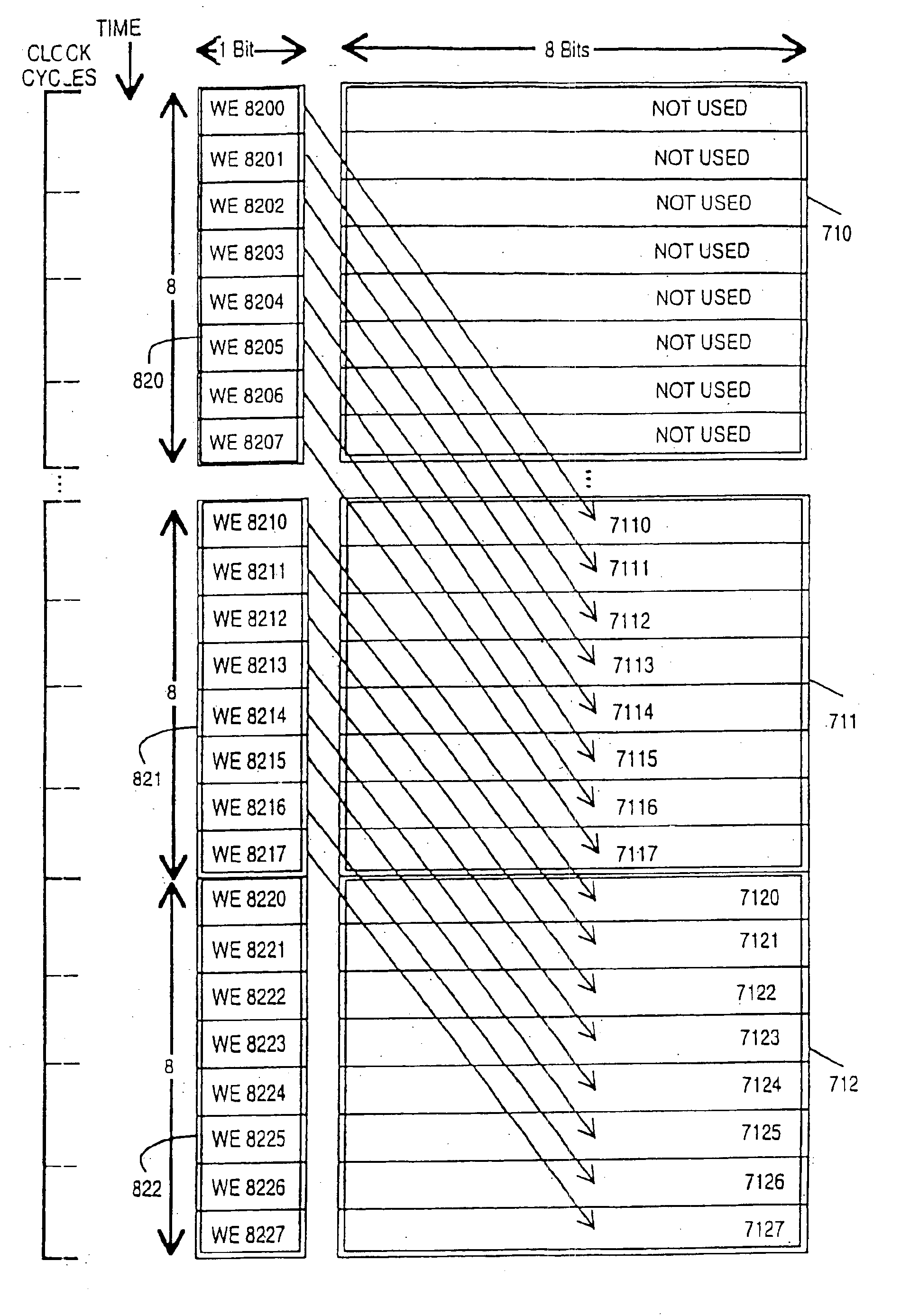
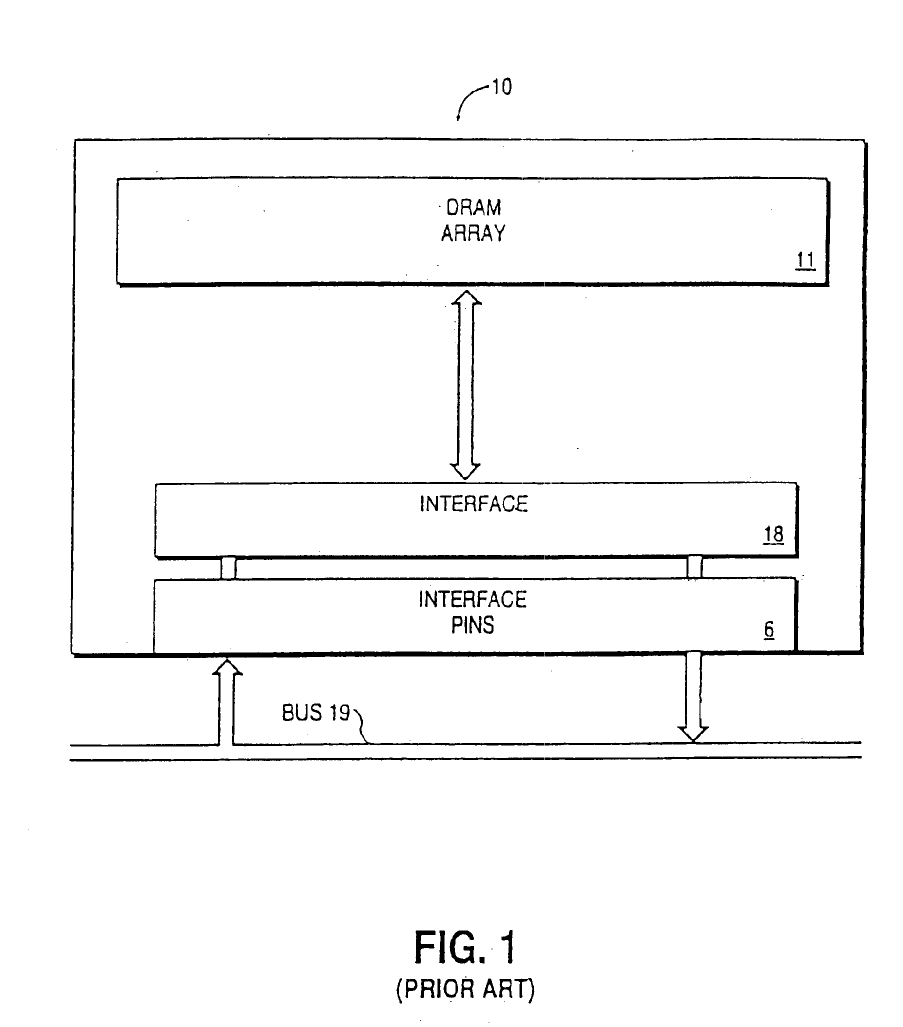
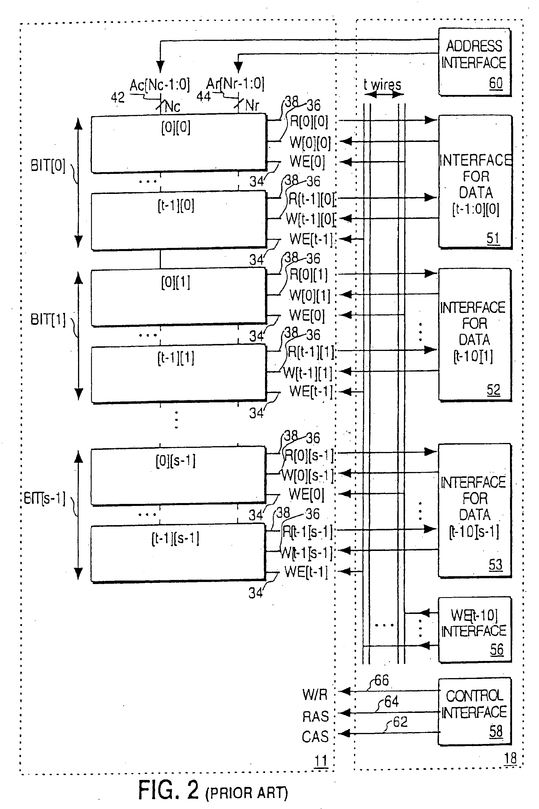
[0054]Configurations are described below that provide a memory with write enable information. The circuit area required is minimized and performance maximized. Embodiments for a DRAM will be described. Alternative embodiments can be implemented with other memory devices, such as SRAM or flash memory. Certain embodiments allow write enable signals to be supplied to the memory in ways that reduce the number of registers required. Certain embodiments allow Write Enable (“WE”) signals, data signals, and Error Detection and Correction (“EDC”) signals to share the same pins, which allows one or more dedicated WE pins to be eliminated. The various embodiments will be described in more detail below.

[0055]FIG. 9 shows computer system 2000 that includes CPU 2004, DRAM master or controller 2002, and sixteen DRAMs 610 through 626. CPU 2004 issues commands to DRAM master 2002. DRAM master 2002 communicates with DRAMs 610 through 626 over high-speed bus 519.

[0056]FIG. 10 is a block diagram of DRA...


PUM


Abstract

A method is described for providing a memory with a serial sequence of write enable signals that are offset in time with respect to respective data received by a plurality of data inputs of the memory. A memory is also described with an array for data storage, a plurality of data input pins, and a separate pin for receiving either additional data or a serial sequence of write enable signals applicable to data received by the plurality of data input pins. The additional data that the separate pin can receive includes, for example, error detection and correction (EDC) information. A method is also described for multiplexing write enable information and error detection and correction information.

Description

[0001]This application is a continuation of U.S. patent application Ser. No. 10 / 147,931 filed May 17, 2002 now U.S. Pat. No. 6,681,288; which is a continuation of U.S. patent application Ser. No. 09 / 966,126, filed Sep. 28, 2001 (now U.S. Pat. No. 6,493,789); which is a continuation of U.S. patent application Ser. No. 09 / 859,097, filed May 14, 2001 (now U.S. Pat. No. 6,496,897); which is a continuation of U.S. patent application Ser. No. 09 / 480,825, filed Jan. 10, 2000 (now U.S. Pat. No. 6,266,737); which is a continuation of U.S. patent application Ser. No. 08 / 545,294, filed Oct. 19, 1995 (now U.S. Pat. No. 6,935,369).FIELD OF THE INVENTION[0002]The present invention relates to the field of electronic memories for data storage. More particularly, the present invention relates to ways of providing a memory with write enable information.BACKGROUND OF THE INVENTION[0003]Digital information can be stored in various types of memories, including random access memories (“RAMs”), electrical...

Claims


Application Information

Patent Timeline
Patent Type & Authority Patents(United States)
IPC IPC(8): G11C7/00G11C7/22G11C11/413G11C11/401
CPCG11C7/22G11C7/00
Inventor WARE, FREDERICK ABBOTTHAMPEL, CRAIG EDWARDSTARK, DONALD CHARLESGRIFFIN, MATTHEW MURDY
Owner RAMBUS INC
Why Eureka
Try Eureka