Construction of an optimized SEC-DED code and logic for soft errors in semiconductor memories

Inactive Publication Date: 2006-10-03
AVAGO TECH WIRELESS IP SINGAPORE PTE
View PDF15 Cites 40 Cited by
  • Summary
  • Abstract
  • Description
  • Claims
  • Application Information

AI Technical Summary

Benefits of technology

[0007]The objects, features and advantages of the present invention include providing a method and/or architecture for construction of an optimized single error correcting and double error detecting (SEC-DED) code and logic for error control coding (ECC) in semiconductor memory that may (i) reduce soft errors, (ii) minimize circuit area, (iii) minimize logic gate count

Problems solved by technology

Semiconductor memories can experience high failure rates due to “soft” errors (i.e., errors where data in a memory array change prior to or during a given memory access and whose original value can be restored upon rewriting of the data).
Causes of soft errors include primarily ionizing radiation effects induced by neutron and alpha particle bombardment and to

Method used


Image

  • Construction of an optimized SEC-DED code and logic for soft errors in semiconductor memories
  • Construction of an optimized SEC-DED code and logic for soft errors in semiconductor memories
  • Construction of an optimized SEC-DED code and logic for soft errors in semiconductor memories

Examples


first embodiment

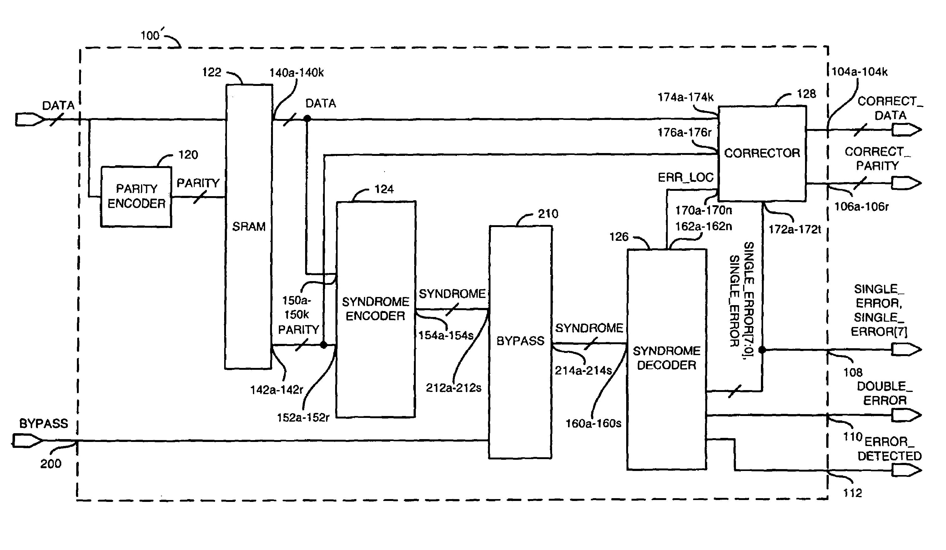
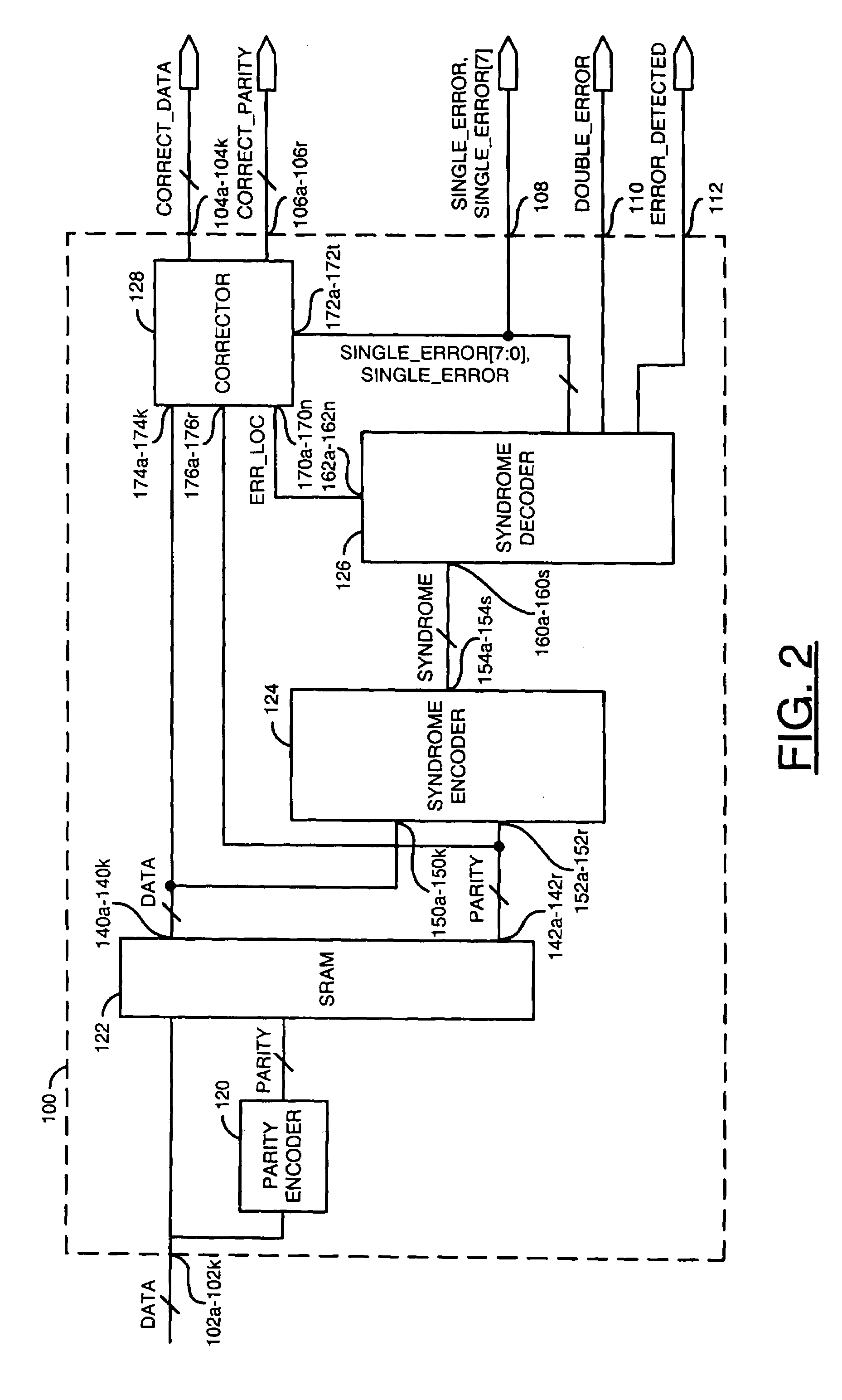
[0053]In a first embodiment, the parity encoder 60 may be implemented as a non-inverting parity encoder using exclusive-OR (e.g., XOR) gates (e.g., alternative 1 in TABLE 1). The non-inverting parity encoder 60 generally presents the parity bits PARITY[0]–PARITY[8] that are the logical combinations of the data bits DATA[0]–DATA[127] generated using XOR logic gates. Each row of the PCM 54 may define the given parity bits PARITY[0]-PARITY[8] generated and the data bits DATA[0]–DATA[127] to be combined to generate the given parity bits PARITY[0]-PARITY[8]. For example, on row 1 of the PCM 54, the parity bit PARITY[0] may be selected as the output. The parity bit PARITY[0] generally corresponds to an ECC parity bit 0. The parity bit PARITY[0] may be equal to an XOR combination of the data bits DATA[0]–DATA[27], DATA[84]–DATA[98], DATA[106], DATA[107], DATA[110], DATA[112], DATA[117], DATA[120], DATA[121], DATA[123], and DATA[127]. The parity bits PARITY[l]-PARITY[8] may be generated sim...

third embodiment

[0055]In a third embodiment, the parity encoder 60 may be implemented as an inverting parity encoder using XOR gates (e.g., alternative 3 in TABLE 1). Each parity bit PARITY[0]-PARITY[8] may be a logical combination of data bits (e.g., DATA[0]–DATA[127]) defined by the PCM 54 and the logic value 1. Any value combined with logic 1 using an XOR gate will generally result in the digital complement (e.g., opposite) of the value. For example, on row 1 of the PCM 54, the parity bit PARITY[0] may be presented as the output. The parity bit PARITY[0] may be equal to the XOR combination of the data bits DATA[0]–DATA[27], DATA[84]–DATA[98], DATA[106], DATA[107], DATA[110], DATA[112], DATA[117], DATA[120], DATA[121], DATA[123], DATA[127] and the logic 1. The parity bits PARITY[1]-PARITY[8] may be generated similarly to the parity bit PARITY[0].

[0056]In a fourth embodiment, the parity encoder 60 may be implemented as an inverting parity encoder using XOR gates with an output inverted by NOT gate...

fifth embodiment

[0070]In a fifth embodiment, the syndrome encoder 62 may be implemented as a non-inverting syndrome encoder using XNOR gates. Each syndrome bit SYNDROME[0]-SYNDROME[8] may be a logical combination of the data bits DATA[0]–DATA[127] and a respective one of the previous parity bits PARITY [0]-PARITY [8] and the logic value 0.

[0071]The fifth embodiment of the syndrome encoder 62 may implement the following two rules to generate the non-inverting syndrome bits SYNDROME[0]-SYNDROME[8]:

[0072]Rule 1: When an odd number of the data bits DATA[0]–DATA[127] and a previous parity bit PARITY[0]-PARITY[8] are presented to the syndrome encoder 62, XNOR logic gates may be implemented to generate the respective syndrome bit SYNDROME [0]-SYNDROME[8]; and / or

[0073]Rule 2: When an even number of the data bits DATA[0]–DATA[127] and a previous parity bit PARITY[0]-PARITY[8] are presented to the syndrome encoder 62, XNOR logic gates may be implemented to combine all of the data bits DATA[0]–DATA[127] prese...


PUM


Abstract

An apparatus for memory error control coding comprising a first circuit and a second circuit. The first circuit may be configured to generate a multi-bit digital syndrome signal in response to a read data signal and a read parity signal. The second circuit may be configured to (i) detect an error when the bits of the syndrome signal are not all the same state and (ii) generate an error location signal in response the syndrome signal. The error location signal may be generated in response to fewer than all of the bits of the syndrome signal.

Description

[0001]This application claims the benefit of U.S. Provisional Application No. 60 / 292,227, filed May 17, 2001 which is hereby incorporated by reference in its entirety.FIELD OF THE INVENTION[0002]The present invention relates to a method and / or architecture for error control coding in semiconductor memory applications generally and, more particularly, to a method and / or architecture for construction of an optimized SEC-DED code and logic for error detection and correction in semiconductor memories.BACKGROUND OF THE INVENTION[0003]Semiconductor memories can experience high failure rates due to “soft” errors (i.e., errors where data in a memory array change prior to or during a given memory access and whose original value can be restored upon rewriting of the data). Causes of soft errors include primarily ionizing radiation effects induced by neutron and alpha particle bombardment and to a much lesser extent due to loss of cell charge, electronic noise, stray radiation, and poor connec...

Claims


Application Information

Patent Timeline
IPC IPC(8): H03M13/00G11C29/00
CPCH03M13/095
Inventor YEUNG, MAX M.STEPHANI, RICHARD J.VILCHIS, MIGUEL A.
Owner AVAGO TECH WIRELESS IP SINGAPORE PTE
Why Eureka
Try Eureka