Ultralow-capacitance TVS device based on SOI material and manufacturing method

An ultra-low capacitance technology, applied in semiconductor/solid-state device manufacturing, electrical components, semiconductor devices, etc., can solve the problems affecting the response time of TVS tubes and insufficient TVS performance, and achieve high operating speed, low power consumption, and reduced leakage Effect

Pending Publication Date: 2021-06-15
傲威半导体无锡有限公司
View PDF0 Cites 0 Cited by
  • Summary
  • Abstract
  • Description
  • Claims
  • Application Information

AI Technical Summary

Problems solved by technology

However, most of the TVS diode devices are still designed on the traditional silicon substrate or epitaxy. There is a certain amount of parasitic capacitance between the traditional silicon wafer and the TVS device. Generally, the parasitic capacitance occurs from I / O to I / O between or I / O to GND
Low-capacitance TVS diodes have particularly high requirements on capacitance. The parasitic capacitance in the body will affect the response time of TVS diodes, which makes the performance of TVS a fly in the ointment.

Method used


Image

  • Ultralow-capacitance TVS device based on SOI material and manufacturing method

Examples


Embodiment Construction

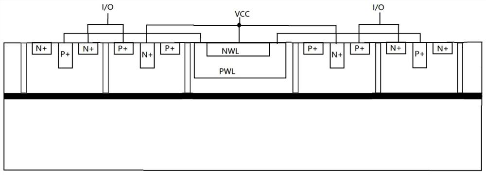
[0035] In order to make the purpose, technical solutions and advantages of the embodiments of the present invention more clear, the technical solutions in the embodiments of the present invention will be clearly and completely described below in conjunction with the drawings in the embodiments of the present invention. Apparently, the described embodiments are some, but not all, embodiments of the present invention. The components of the embodiments of the invention generally described and illustrated in the figures herein may be arranged and designed in a variety of different configurations. Accordingly, the following detailed description of the embodiments of the invention provided in the accompanying drawings is not intended to limit the scope of the claimed invention, but merely represents selected embodiments of the invention. Based on the embodiments of the present invention, all other embodiments obtained by persons of ordinary skill in the art without creative efforts ...


PUM

PropertyMeasurementUnit
depthaaaaaaaaaa
widthaaaaaaaaaa
depthaaaaaaaaaa

Abstract

The invention provides an ultralow-capacitance TVS device based on an SOI material and a manufacturing method. The TVS device comprises a substrate layer which is made of an SOI silicon wafer; an N well / P well / N+ / P+ region which is formed on the substrate layer and forms a TVS; an N+ / P+ region which is formed on the substrate layer and forms a switching tube; a surface shallow groove which is formed in the N+ / P+ region and surrounds between an N+ region and a P+ region, wherein the junction depth of the surface shallow groove is smaller than that of the N+ / P+ region; a shallow slot filling layer which adopts an oxide layer and is formed in the surface shallow groove; a surface deep groove which is formed in the substrate layer and isolates the N well / P well / N+ / P+ region from the N+ / P+ region; a deep groove filling layer which adopts an oxide layer and is formed in the surface deep groove; and an electrode which is formed on the surface of the wafer and is led out through multiple layers of metallization. The parasitic capacitance is reduced, the operation speed is improved, and the power consumption is lower.

Description

technical field [0001] The invention relates to a transient suppression diode, in particular to an ultra-low capacitance TVS device based on SOI material and a manufacturing method. Background technique [0002] Low-capacitance TVS diodes are used to protect sensitive electronic equipment from high surges, and become ideal circuit passive protection components in high-speed Ethernet communication lines, high-speed interfaces in industrial applications, and automotive electronics. At the same time, due to the unique low leakage current advantages of low-capacitance transient TVS diodes, they have been widely used in the field of high-speed communication, which helps to improve the CAN system of vehicle electronics, security monitoring equipment, smart home, Internet of Things sensors and other products. power efficiency and extend operating time. However, most of the TVS diode devices are still designed on the traditional silicon substrate or epitaxy. There is a certain amou...

Claims


Application Information

Patent Timeline
Patent Type & Authority Applications(China)
IPC IPC(8): H01L29/861H01L29/06H01L21/329
CPCH01L29/0603H01L29/0684H01L29/6609H01L29/861
Inventor 陆亚斌吴昊王成
Owner 傲威半导体无锡有限公司
Why Eureka
Try Eureka