Hybrid orientation field effect transistors (FETs)

a field effect transistor and hybrid technology, applied in the field of hybrid orientation fets, can solve the problems of increasing the difficulty of vt control and serious fluctuations of dopan

Inactive Publication Date: 2006-09-05
DATALOGIC IP TECH +1
View PDF14 Cites 28 Cited by
  • Summary
  • Abstract
  • Description
  • Claims
  • Application Information

AI Technical Summary

Benefits of technology

[0007]The present invention also provides a hybrid orientation semiconduct

Problems solved by technology

Dopant fluctuations are becoming a serious problem in Vt (threshold voltage) control in advanced semiconductor devices.
As semiconductor devices

Method used


Image

  • Hybrid orientation field effect transistors (FETs)
  • Hybrid orientation field effect transistors (FETs)
  • Hybrid orientation field effect transistors (FETs)

Examples


Embodiment Construction

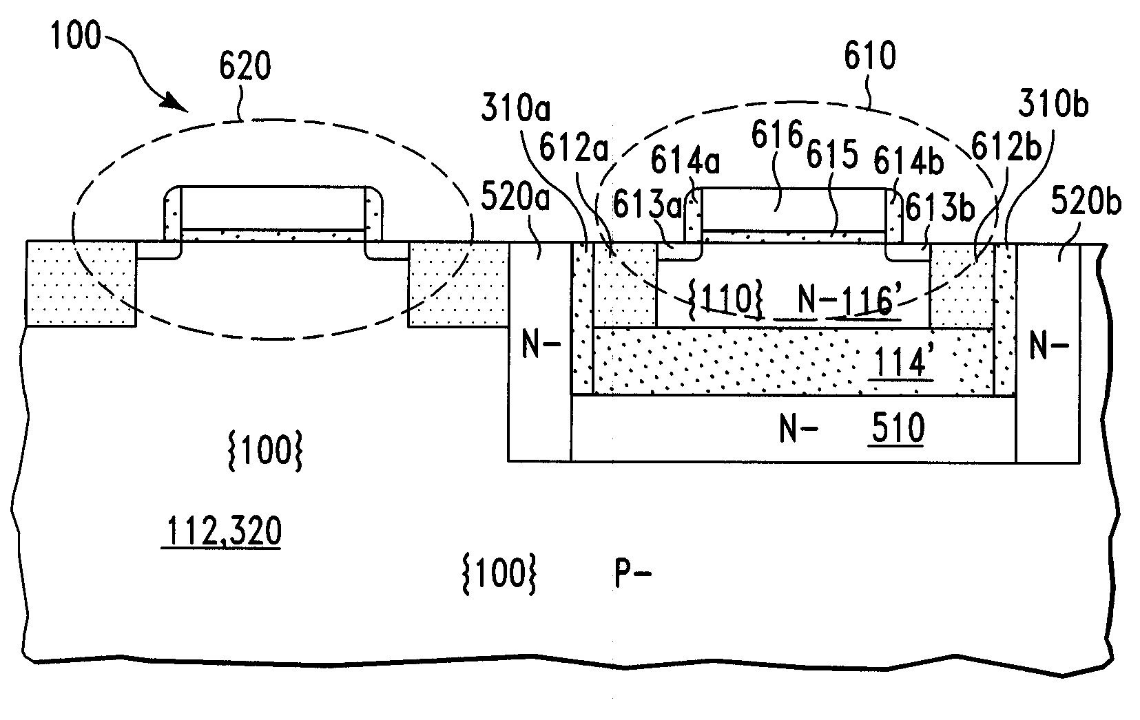
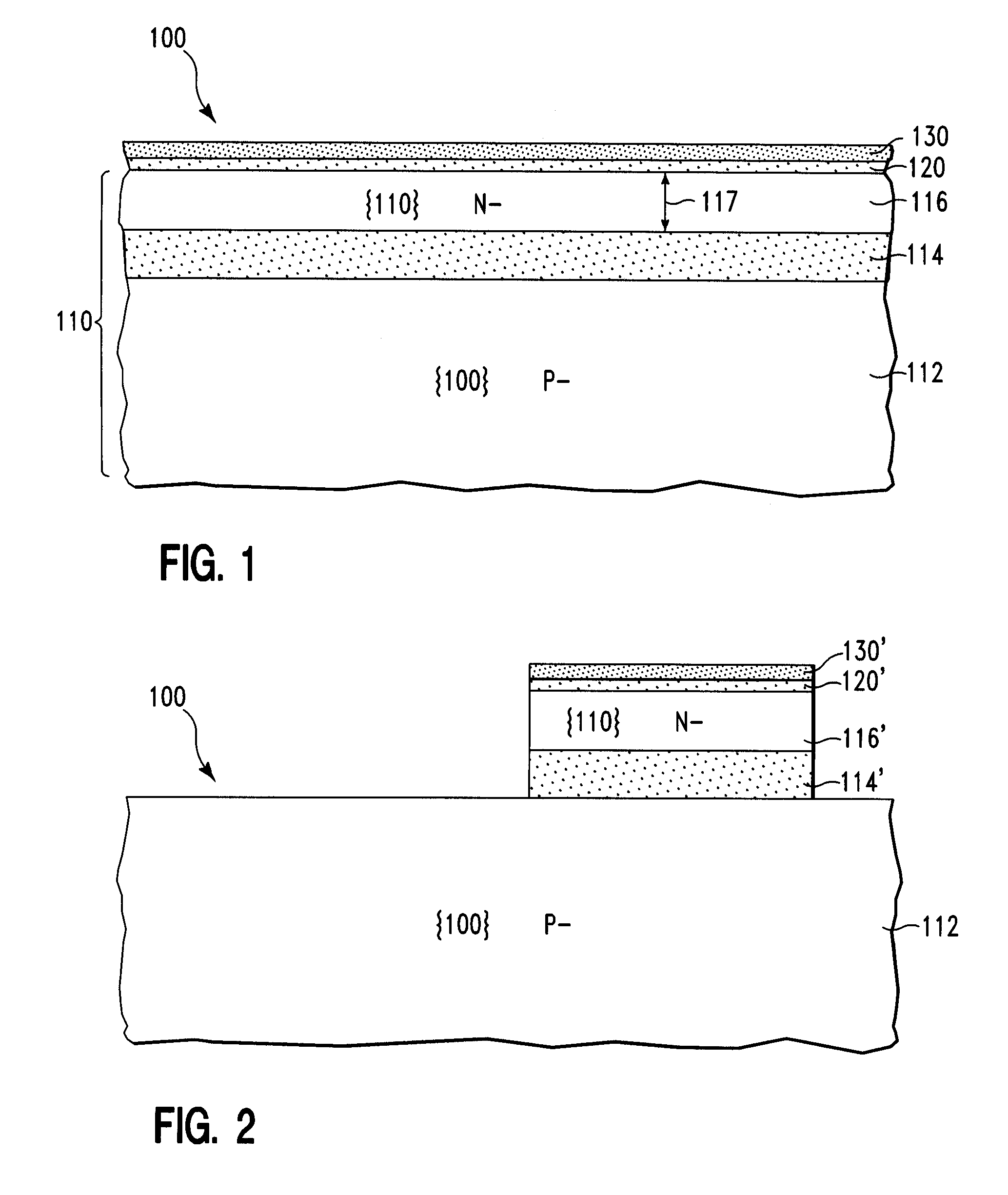
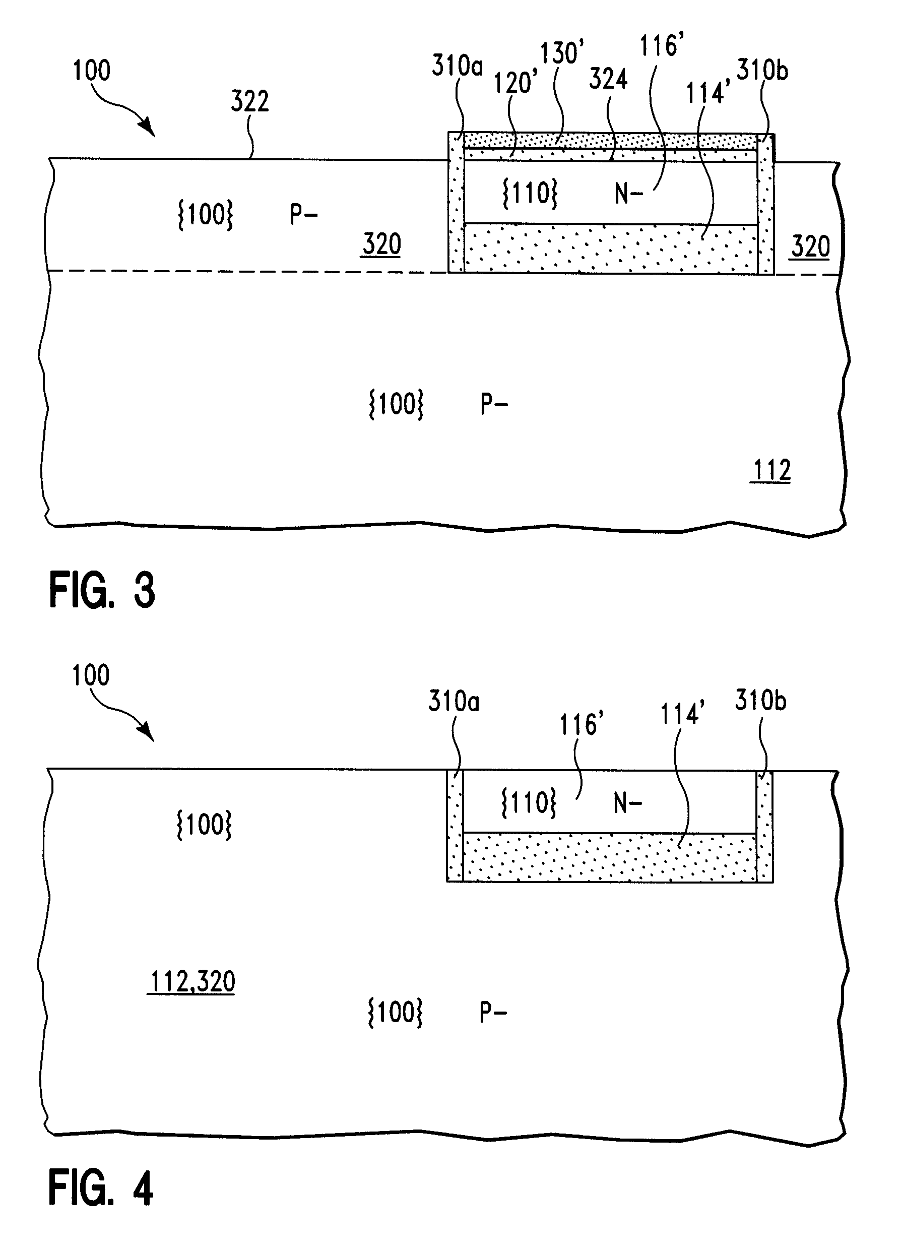
[0010]FIGS. 1–8 illustrate cross-section views of a hybrid orientation semiconductor structure 100 going through different fabrication steps, in accordance with embodiments of the present invention. More specifically, with reference to FIG. 1, in one embodiment, the fabrication of the structure 100 starts out with a silicon on insulator (SOI) substrate 110. The SOI substrate 110 comprises a bottom silicon layer 112, a buried oxide (BOX) layer 114, and a top silicon layer 116.

[0011]The bottom silicon layer 112 is lightly doped P type (i.e., doped with P type dopants such as Boron atoms) and have lattice orientation {100}, whereas the top silicon layer 116 is lightly doped N type (i.e., doped with N type dopants such as phosphorous atoms) and have lattice orientation {110}. The minus signs in “P−” and “N−” as used in the figures indicate lightly doped. The BOX layer 114 comprises a dielectric material such as silicon dioxide.

[0012]In one embodiment, the SOI substrate 110 is formed usi...


PUM


Abstract

A hybrid orientation semiconductor structure and method of forming the same. The structure includes (a) a semiconductor substrate comprising a first semiconductor material having a first lattice orientation; (b) a back gate region on the semiconductor substrate; (c) a back gate dielectric layer on the back gate region; (d) a semiconductor region on the back gate dielectric layer, wherein the semiconductor region is electrically insulated from the back gate region by the back gate dielectric layer, and wherein the semiconductor region comprises a second semiconductor material having a second lattice orientation different from the first lattice orientation; and (e) a field effect transistor (FET) formed on the semiconductor region, wherein changing a voltage potential applied to the back gate region causes a change in a threshold voltage of the FET.

Description

BACKGROUND OF THE INVENTION[0001]1. Technical Field[0002]The present invention relates to field effect transistors (FETs), and more specifically, to hybrid orientation FETs.[0003]2. Related Art[0004]Dopant fluctuations are becoming a serious problem in Vt (threshold voltage) control in advanced semiconductor devices. As semiconductor devices become smaller and smaller in size, Vt control becomes more difficult. Hybrid orientation field effect transistors (FETs) have the same problems. As a result, there is a need for a hybrid orientation semiconductor structure (and methods for forming the same) that allows for Vt control.SUMMARY OF THE INVENTION[0005]The present invention provides a semiconductor structure, comprising (a) a semiconductor substrate comprising a first semiconductor material having a first lattice orientation; (b) a back gate region on the semiconductor substrate; (c) a back gate dielectric layer on the back gate region; (d) a semiconductor region on the back gate die...

Claims


Application Information

Patent Timeline
IPC IPC(8): H01L29/04H01L27/12
CPCH01L21/823807H01L21/823828H01L21/823878H01L27/1203H01L27/0922H01L27/1207H01L29/045H01L21/84
Inventor BRYANT, ANDRESCLARK, JR., WILLIAM F.NOWAK, EDWARD J.
Owner DATALOGIC IP TECH
Why Eureka
Try Eureka