Thin-film electrode layer including beta-ta and thin-film magnetic head using the same

a thin-film electrode and magnetic head technology, applied in the field of thin-film electrode layers, can solve the problems of above-described conventional ta/au/ta electrode structure with em resistance, and achieve the effect of reducing the resistance of the thin-film electrode layer

Inactive Publication Date: 2006-09-05
ALPS ALPINE CO LTD
View PDF6 Cites 4 Cited by
  • Summary
  • Abstract
  • Description
  • Claims
  • Application Information

AI Technical Summary

Benefits of technology

[0009]This structure inhibits a resistance change in the main conductive layer due to the, presence of the second base sublayer. Moreover, the resistivity of the second base sublayer is decreased by the presence of the first base sublayer.
[0013]According to the method, each end portion of the thin-film electrode layer near the magnetoresistive element M can have a sufficient thickness, and the layers at the end portions can be sufficiently adhered to each otherwhich allows the resistance of the thin-film electrode layers to be effectively decreased.

Problems solved by technology

However, the above-described conventional Ta / Au / Ta electrode structure has a problem with electromigration (EM) resistance.

Method used


Image

  • Thin-film electrode layer including beta-ta and thin-film magnetic head using the same
  • Thin-film electrode layer including beta-ta and thin-film magnetic head using the same
  • Thin-film electrode layer including beta-ta and thin-film magnetic head using the same

Examples


first embodiment

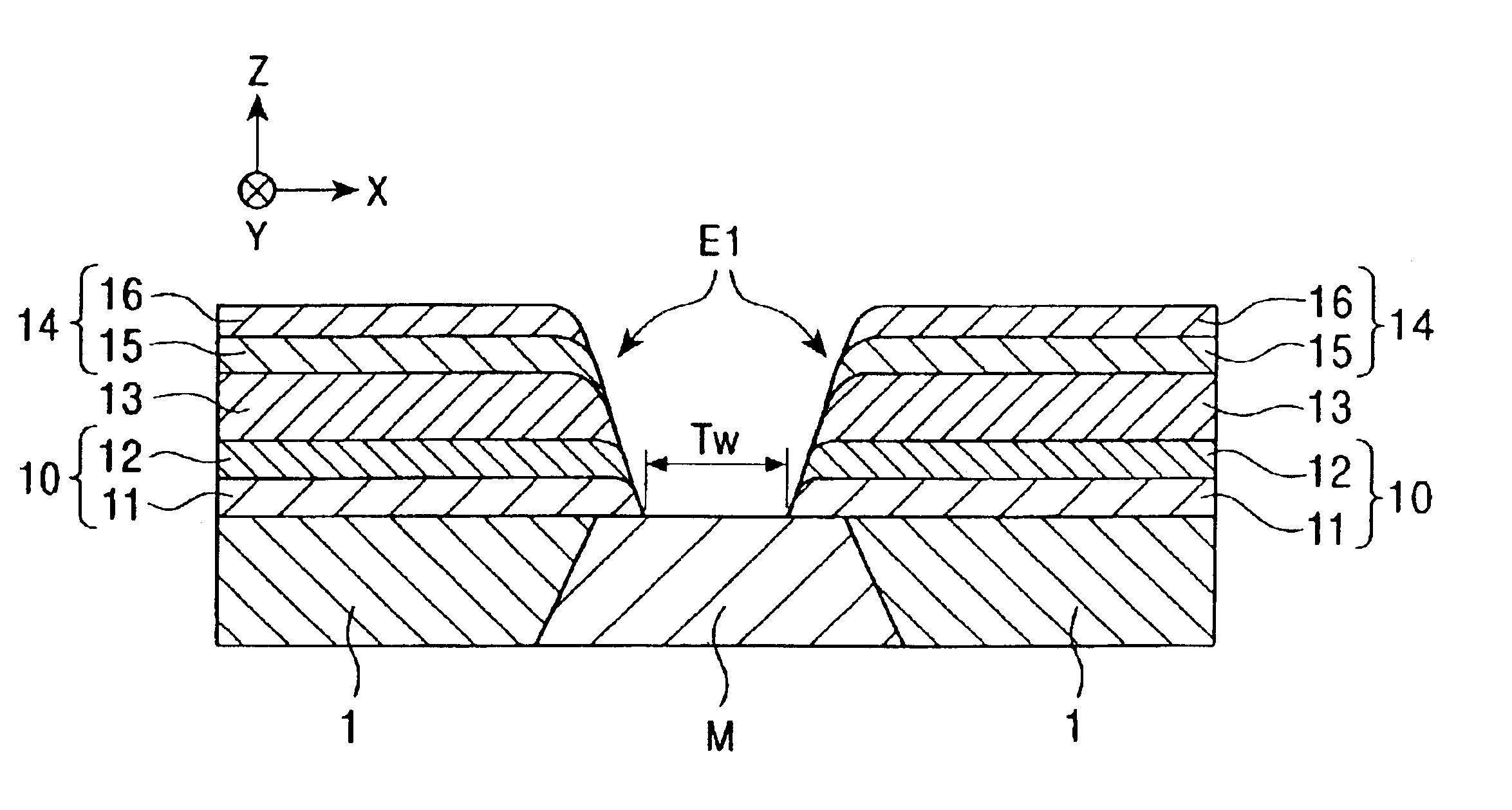
[0048]FIG. 1 is a schematic cross-sectional view of the structure of thin-film electrode layers E1 according to a first embodiment of the present invention when viewed from the face that opposes a recording medium. Each of the thin-film electrode layers E1 is formed by stacking metal layers and is constituted from a base layer 10 disposed on the permanent magnet layer 1 and part of the magnetoresistive element M; a main conductive layer 13 composed of gold; and a protective layer 14 formed on the main conductive layer 13. The base layer 10 prevents the diffusion of the main conductive layer 13. The protective layer 14 prevents smearing, i.e., sagging, of the main conductive layer 13 that occurs during polishing the X-Z plane, which is the recording-medium opposing face. When smearing of the main conductive layer 13 is prevented using the protective layer 14, the upper shield layer (not shown) stacked on the top of the thin-film electrode layer E1 with the insulating layer therebetwe...

second embodiment

[0055]FIG. 7 is a schematic cross-sectional view showing the structure of thin-film electrode layers E2 according to a second embodiment of the present invention viewed from the face opposing a recording medium. The second embodiment differs from the first embodiment in that the protective layer 14 is constituted from a β-Ta sublayer 17 and a Cr sublayer 15. Other structures are the same as those of the first embodiment. In other words, the second embodiment also has an electrode structure formed by stacking the first base sublayer 11, the second base sublayer 12, and the main conductive layer 13. In FIG. 7, the constituent elements are substantially the same as those of the first embodiment and are represented by the same reference characters.

[0056]The thin-film electrode layers E2 are comprised of a first base sublayer 11 composed of β-Ta, a second base sublayer 12 composed of Cr, a main conductive layer 13 composed of Au, a β-Ta sublayer 17, and a Cr sublayer 15, stacked in that ...

third embodiment

[0061]FIG. 16 is a schematic cross-sectional view showing the structure of thin-film electrode layers E3 according to a third embodiment of the present invention viewed from the face opposing a recording medium. The third embodiment is substantially the same as the first embodiment except that the protective layer 14 is comprised of only the Cr sublayer 15. In FIG. 16, the constituent elements are substantially the same as those of the first embodiment and are represented by the same reference characters.

[0062]The thin-film electrode layers E3 are comprised of a first base sublayer 11 composed of β-Ta, a second base sublayer 12 composed of Cr, a main conductive layer 13 composed of Au, and a protective layer 14 comprised of a Cr sublayer 15, stacked in that order on the magnetoresistive element M and the permanent magnet layers 1. Smearing of the main conductive layer 13 can be effectively prevented even when the protective layer 14 is constituted from only the Cr sublayer 15.

[0063]...


PUM

PropertyMeasurementUnit
volume resistivityaaaaaaaaaa
currentaaaaaaaaaa
conductiveaaaaaaaaaa

Abstract

A thin-film electrode layer having a superior electromigration resistance is disclosed. The thin-film electrode layer includes a first base layer composed of β-Ta, a main conductive layer composed of Au, and a protective layer. The protective layer is a composite of a Cr sublayer and an α-Ta sublayer. A thin-film magnetic head having the thin-film electrode layers and a method for forming electrodes in the thin-film magnetic head are also disclosed.

Description

BACKGROUND OF THE INVENTION[0001]1. Field of the Invention[0002]The present invention relates to a thin-film electrode layer for supplying an electric current to a magnetoresistive element, a thin-film magnetic head using a thin-film electrode layer, and a method for forming electrodes in a thin-film magnetic head.[0003]2. Description of the Related Art[0004]Thin film magnetic heads having magnetoresistive elements include thin-film electrode layers for supplying electric current to the magnetoresistive elements. When electric current is supplied to a magnetoresistive element, the resistance of the magnetoresistive element changes, and a leakage magnetic field from a recording medium can be detected by a change in voltage due to a change in resistance. The thin-film magnetic head preferably has thin-film electrode layers composed of a metal having a small resistivity, such as gold, so as to reduce the electrical resistance of components other than the magnetoresistive element.[0005]...

Claims


Application Information

Patent Timeline
Patent Type & Authority Patents(United States)
IPC IPC(8): G11B5/33G11B5/00G11B5/31G11B5/39H01F10/06H01L43/08
CPCG11B5/3932G11B5/3903G11B5/313G11B5/3163Y10T29/49052
Inventor TAKAHASHI, AKIRATAKAHASHI, JUNKAWASAKI, YUKOHONDA, KENJIISHIBASHI, NAOHIROUMETSU, EIJI
Owner ALPS ALPINE CO LTD
Why Eureka
Try Eureka