
Infrared ray sensor using silicon oxide film as infrared ray absorption layer and method of fabricating the same

a silicon oxide film and infrared ray absorption technology, applied in the field of infrared ray sensors, can solve the problems of reducing process yield and disadvantageous portion of substrates, and achieve the effects of improving infrared ray absorption capability, reducing manufacturing processes, and robust structur

Active Publication Date: 2006-09-12
INTELLECTUAL DISCOVERY CO LTD
View PDF16 Cites 6 Cited by
  • Summary
  • Abstract
  • Description
  • Claims
  • Application Information

AI Technical Summary

Benefits of technology

The present invention is an infrared ray sensor that has a strong structure, reduces fabrication processes, and improves infrared ray absorption in the 8 to 12 mm wavelength band. It includes a focal plate with an infrared ray absorption layer, support arms, and posts integrated in a single body using silicon oxide films. The sensor has a simple fabrication process and is highly sensitive to infrared rays. The technical effects of the invention include improved infrared ray absorption, reduced fabrication processes, and a simplified structure.

Problems solved by technology

Therefore, such a configuration is structurally unstable, so that the process yield decreases.
In addition, the top portion of the substrate must disadvantageously have a metallic thin film which functions as a reflecting mirror for reflecting the incident infrared ray from the substrate.

Method used


Image

  • Infrared ray sensor using silicon oxide film as infrared ray absorption layer and method of fabricating the same
  • Infrared ray sensor using silicon oxide film as infrared ray absorption layer and method of fabricating the same
  • Infrared ray sensor using silicon oxide film as infrared ray absorption layer and method of fabricating the same

Examples


Embodiment Construction

[0024]The present invention will be described in detail by way of a preferred embodiment with reference to accompanying drawings, in which like reference numerals are used to identify the same or similar parts.

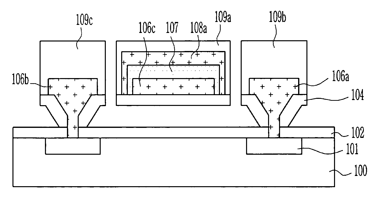
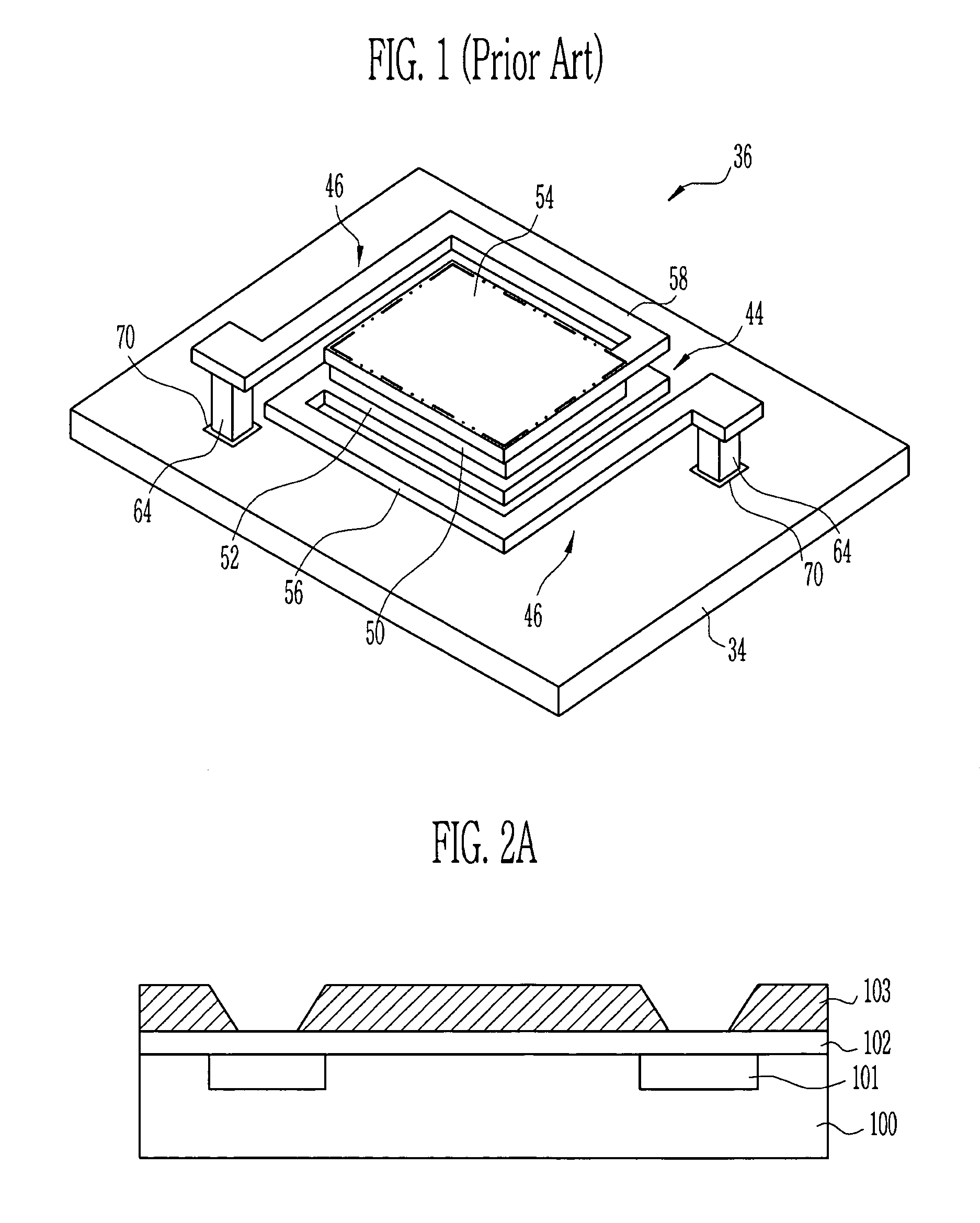
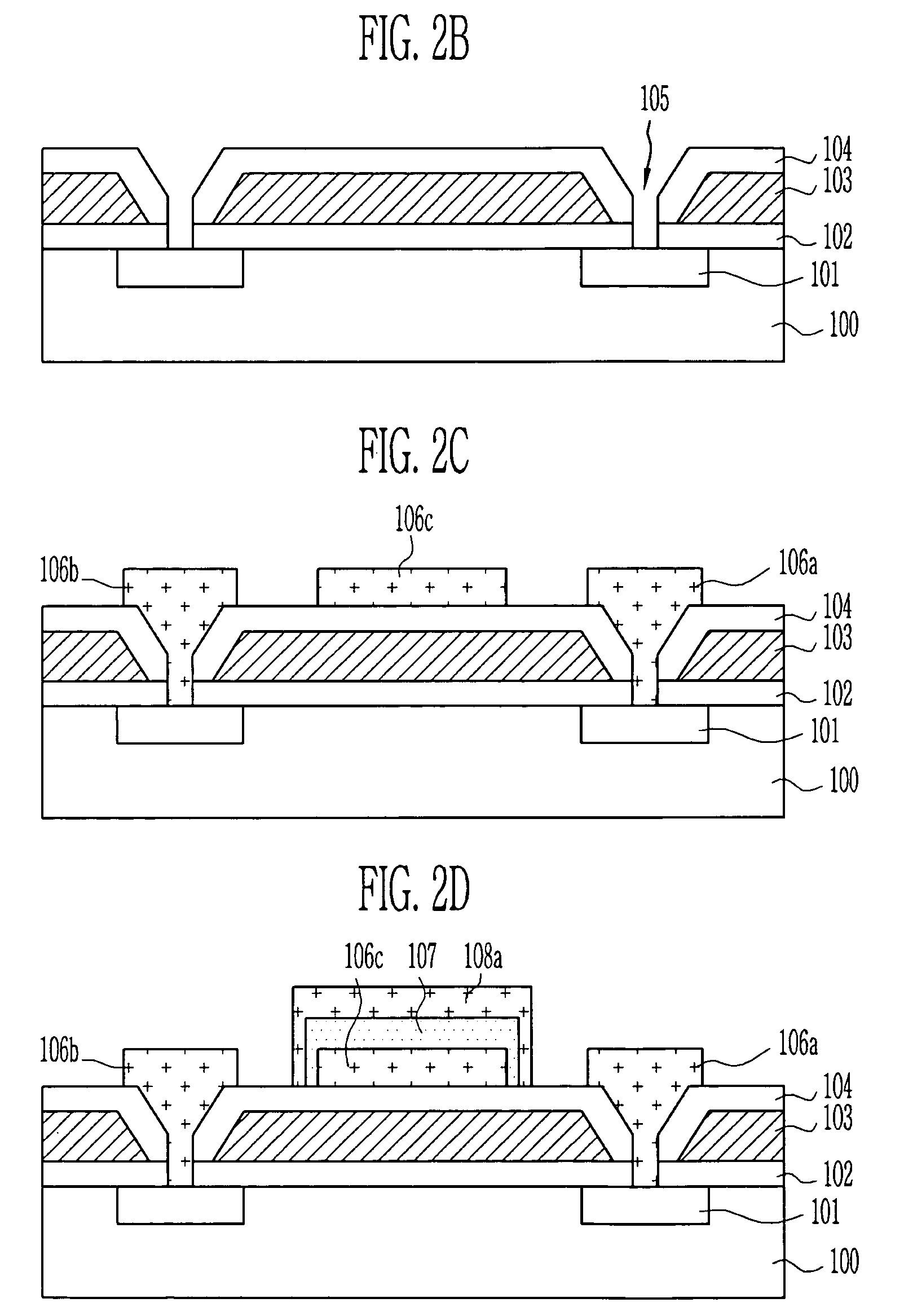
[0025]FIGS. 2A to 2F are cross sectional views for explaining a method of fabricating an infrared ray sensor according to a preferred embodiment of the present invention, and FIG. 3 is a plan view for explaining FIGS. 2C to 2E. The figures illustrate schematic cross sectional structures and a plane structure for explaining an embodiment of the present invention.

[0026]Referring to FIG. 2A, a protective film 102 and a sacrificial layer 103 are sequentially formed on a substrate 100 in which a predetermined circuitry pattern (not shown) and at least two junctions 101 are formed, and then the sacrificial layer 103 is patterned to expose a part of the protective film 102 on the top portion of the junction 101. The protective film 102 is formed with an oxide film having a thickness ...


PUM


Abstract

The present invention relates to a pyroelectric infrared ray sensor fabricated by using MEMS processes, wherein an infrared ray absorption layer disposed on the most top portion of the infrared ray sensor assembly is formed with a silicon oxide film (SiO2) to exhibit an excellent absorption efficiency with respect to the infrared wavelength band of 8 to 12 mm and function as a protective film for a sensor pixel. In addition, an infrared ray absorption layer, support arms and posts are formed in a single body to allow the sensor assembly to be robust and fabricating processes to be remarkably reduced to increase a process yield.

Description

BACKGROUND[0001]1. Field of the Invention[0002]The present invention relates to an infrared ray sensor and, more particularly, to an uncooled pyroelectric infrared ray sensor in which an infrared ray absorption layer of a focal plate is composed of a silicon oxide film, and the infrared ray absorption layer, support arms and posts are integrated in a single body, and a method of fabricating the same.[0003]2. Discussion of Related Art[0004]A focal plate of a pyroelectric infrared ray sensor is an element that converts an incident infrared energy into a thermal energy to transmit it to a pyroelectric thin film and detects the variation of charges generated in a pyroelectric material at the same time as an electrical signal. Typically, a focal plate of an infrared ray sensor includes several parts such as a part for converting an incident infrared ray into a thermal energy, a part of the functional material for exhibiting differences of the electrical characteristics in accordance with...

Claims


Application Information

Patent Timeline
Patent Type & Authority Patents(United States)
IPC IPC(8): G01J5/00H01L31/09G01J5/10G01J5/34
CPCG01J5/02G01J5/023G01J5/34G01J5/0853G01J5/10G01J5/08H01L31/09
Inventor RYU, SANG OUKCHO, SEONG MOKKIM, KWI DONGYU, BYOUNG GON
Owner INTELLECTUAL DISCOVERY CO LTD
Learn More