Inspection device and inspection method for active matrix panel, and manufacturing method for active matrix organic light emitting diode panel

Inactive Publication Date: 2006-09-12
IBM CORP
View PDF5 Cites 75 Cited by
  • Summary
  • Abstract
  • Description
  • Claims
  • Application Information

AI Technical Summary

Benefits of technology

[0023]In addition, the inspection process can estimate the parasitic capacitance on each line of the inspection wiring while setting the driving TFT of a pixel subjected to AC coupling directly with the relevant line of the inspection wiring to an on state, and thereby estimate the number of the pixels having open defects in the driving TFTs thereof by use of a difference between a maximum value of the estimated parasitic capacitance and the individual parasitic capacitance. Moreover, the inspection process can estimate the parasitic capacitance on each line of the inspection wiring while setting the driving TFT of the pixel subjected to AC coupling directly with the relevant line of the inspection wiring to an o

Problems solved by technology

Although there are at least two TFTs in the pixel circuit of the TFT array substrate in the AMOLED, it is impossible to conduct an electric current on the driving TFT only by input and output from a panel interface terminal.
Accordingly, it is not possible to inspect open/short defects in the driving TFT 302 only by input and output to/from the panel interface terminal.
As a result, it is not possible to perform open/short measurement of the driving TFT 302 set to the open-drain (or open-source) state by use of the known techniques.
However, this technique is not designed to perform

Method used


Image

  • Inspection device and inspection method for active matrix panel, and manufacturing method for active matrix organic light emitting diode panel
  • Inspection device and inspection method for active matrix panel, and manufacturing method for active matrix organic light emitting diode panel
  • Inspection device and inspection method for active matrix panel, and manufacturing method for active matrix organic light emitting diode panel

Examples


Embodiment Construction

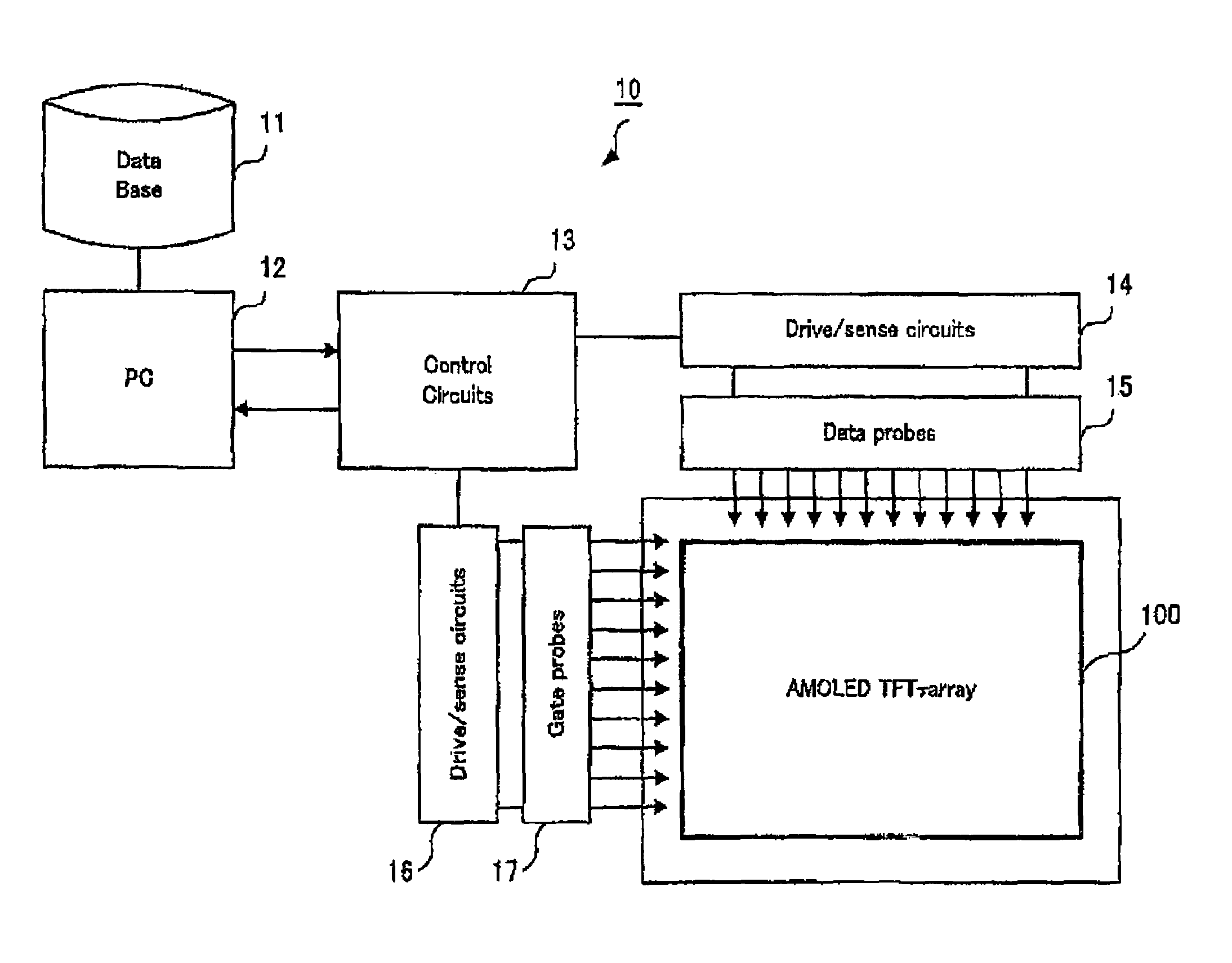
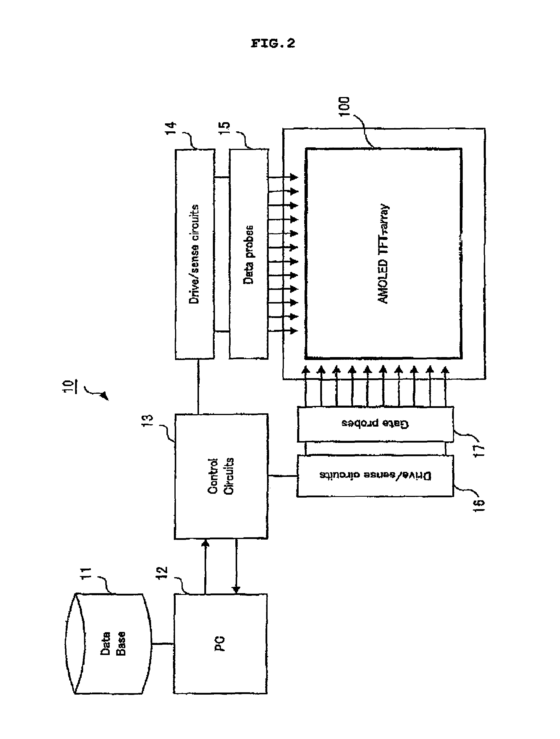
[0042]Now, the present invention will be described in detail based on an embodiment with reference to the accompanying drawings.

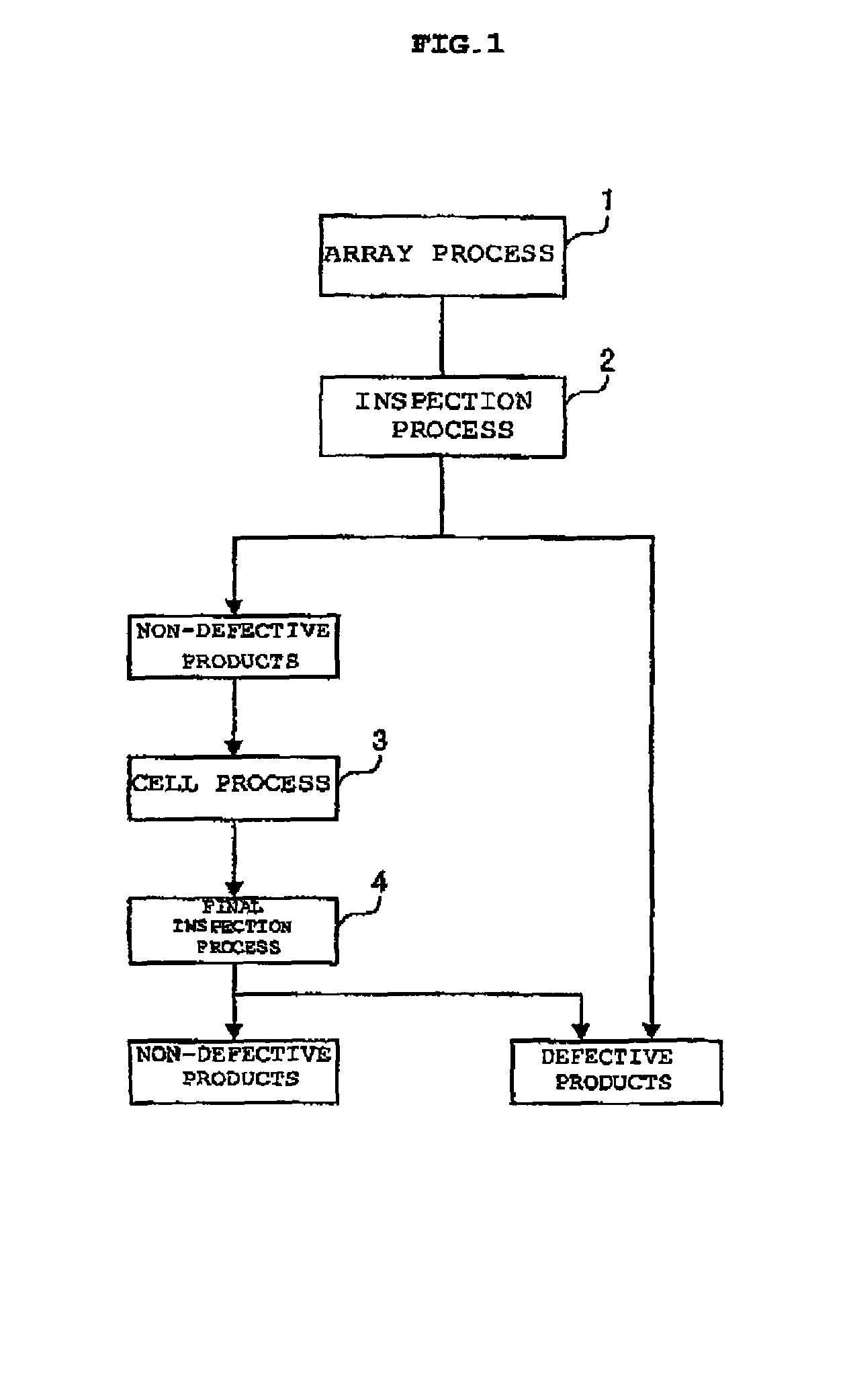
[0043]FIG. 1 is a view for explaining a manufacturing process of an OLED panel in accordance with an embodiment of the present invention. The manufacturing method includes an array process 1 of fabricating a thin film transistor (TFT) array (an active matrix panel) which is a driving circuit for the OLED, and an inspection process 2 of carrying out a performance test on the independent TFT array thus fabricated. The inspection process 2 checks whether open / short defects of wiring are below a predetermined condition and whether characteristics of the driving TFTs constituting the TFT array are uniform throughout the panel. A TFT array judged as a defective product in this inspection process 2 will not be forwarded to a subsequent process but removed instead. A TFT array judged as a non-defective product will be forwarded to a cell process 3 of forming the OL...


PUM


Abstract

An inspection method includes an array process of forming a TFT array on a substrate to fabricate an active matrix panel, an inspection process of carrying out a performance test on the fabricated active matrix panel, and a cell process of mounting an OLED on the active matrix panel after the inspection process. In the inspection process, variation in parasitic capacitance through a pixel electrode is measured when driving TFTs constituting the active matrix fabricated in the array process are turned on and when the driving TFTs are turned off, and open/short defects in the driving TFTs are thereby inspected.

Description

FIELD OF THE INVENTION[0001]The present invention relates to an inspection device and the like for an active matrix organic light emitting diode (OLED) panel, and more specifically to an inspection device and the like for conducting performance inspection of a thin film transistor (TFT) array prior to an OLED formation process.BACKGROUND[0002]An OLED (also referred to as organic electro luminescence (EL)) is for conducting a direct current on a fluorescent organic compound which is excited by application of an electric field, and thereby causing light emission of the compound. The OLED is drawing attention as a next-generation display device in terms of low-profileness, a wide view angle, and a wide gamut, etc. Whereas a driving method for the OLED includes a passive type and an active type, the active type is suitable for achieving a large-screen and high-definition display in light of aspects involving a material, a life, and crosstalks. This active type requires thin film transis...

Claims


Application Information

Patent Timeline
IPC IPC(8): G01R31/00H05B33/10G01R27/26G01R31/26G09F9/00G09F9/30G09G3/00G09G3/32H01L21/66H01L27/32H01L29/786H01L51/50H05B33/14
CPCG09G3/006G09G2330/10G09G2300/0842G09G3/3225
Inventor NAKANO, DAIJUSAKAGUCHI, YOSHITAMI
Owner IBM CORP
Why Eureka
Try Eureka