Method of inspecting optical waveguide substrate for optical conduction at increased speed and also inspecting optical waveguide substrate for crosstalk

a technology of optical waveguide and substrate, which is applied in the direction of testing fibre optic/optical waveguide devices, instrumentation, and measurement of structures/machines, can solve the problems of difficult inspection of cross-talk and difficulty in inspection cross-talk, and achieve the effect of simple arrangement and increased inspection ra

Inactive Publication Date: 2006-09-12
NEC TOPPAN CIRCUIT SOLUTIONS
View PDF2 Cites 0 Cited by
  • Summary
  • Abstract
  • Description
  • Claims
  • Application Information

AI Technical Summary

Benefits of technology

[0011]To achieve the above object, there is provided a method of inspecting an optical waveguide substrate by applying a laser beam to one end face of an optical waveguide of the optical waveguide substrate which is an object to be inspected, detecting the laser beam emitted from the other end of the optical waveguide with an imaging camera to output detected image information, thereafter comparing the detected image information with stored reference image information to inspect the optical waveguide substrate. The method makes it possible to determine whether the conduction of the laser beam through the optical waveguide is acceptable or not and whether cross-talk in the optical waveguide is acceptable or not. Consequently, the optical waveguide can be inspected at an increased inspecting rate and can be inspected for cross-talk.
[0012]According to the present invention, there is also provided a method of inspecting a mounted optical component by reflecting a laser beam emitted from an inspecting optical waveguide on an optical waveguide substrate from the mounted optical component, and detecting the returned amount of reflected light of the laser beam to inspect a positional displacement of the mounted optical component. Therefore, a positional displacement of the mounted optical component can be inspected with a simple arrangement.

Problems solved by technology

Furthermore, because the light beams emitted from the respective unit cells of optical waveguide array 101 are detected altogether by light detector 106, it is difficult to inspect cross-talk.
According to the above conventional inspecting method, inasmuch as the light beams emitted from the respective unit cells of optical waveguide array 101 are detected altogether by light detector 106, as shown in FIG. 1, it is unable to distinguish the light beams emitted from the individual unit cells from each other, resulting in difficulty to inspect cross-talk.

Method used


Image

  • Method of inspecting optical waveguide substrate for optical conduction at increased speed and also inspecting optical waveguide substrate for crosstalk
  • Method of inspecting optical waveguide substrate for optical conduction at increased speed and also inspecting optical waveguide substrate for crosstalk
  • Method of inspecting optical waveguide substrate for optical conduction at increased speed and also inspecting optical waveguide substrate for crosstalk

Examples


1st embodiment

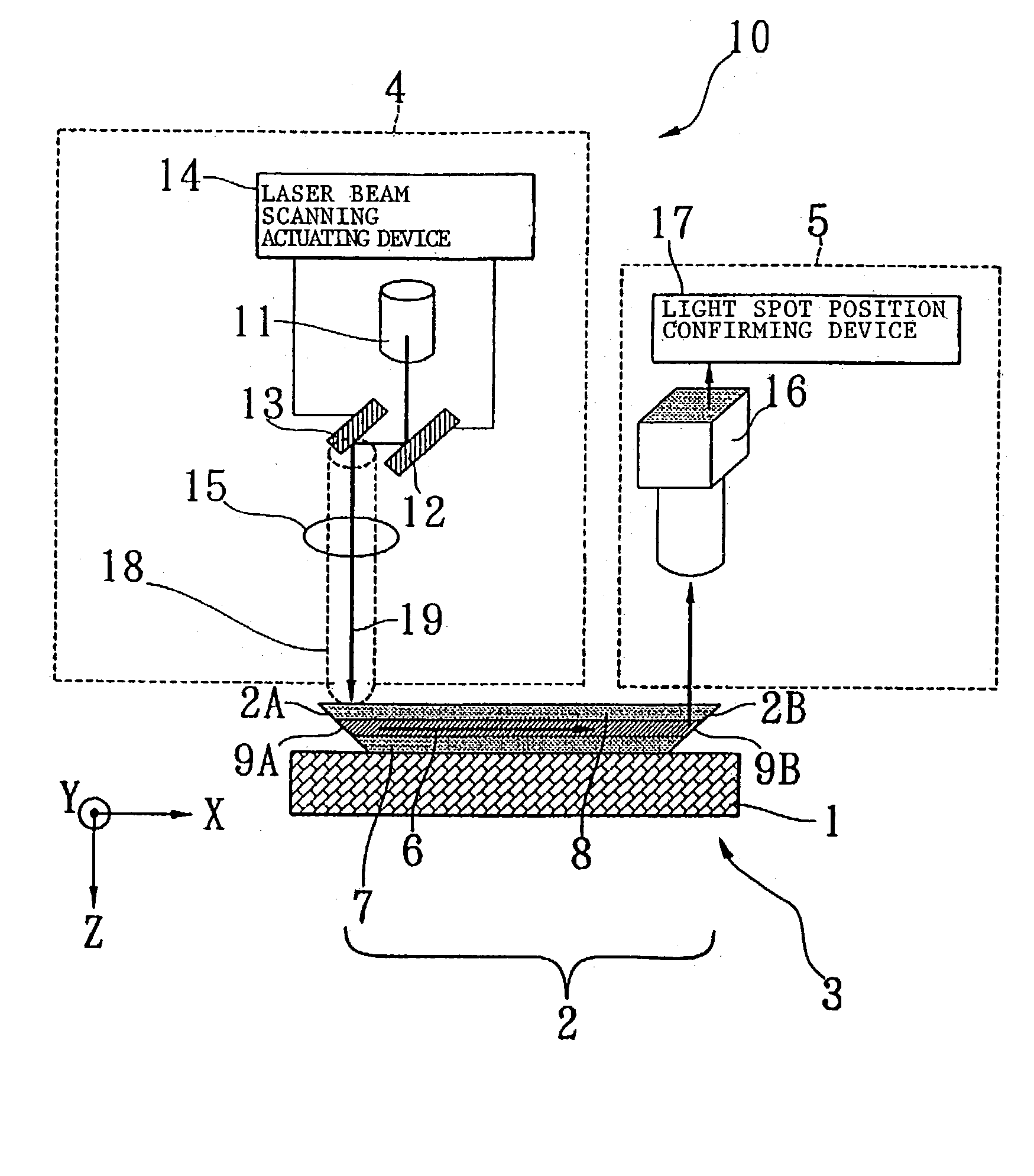
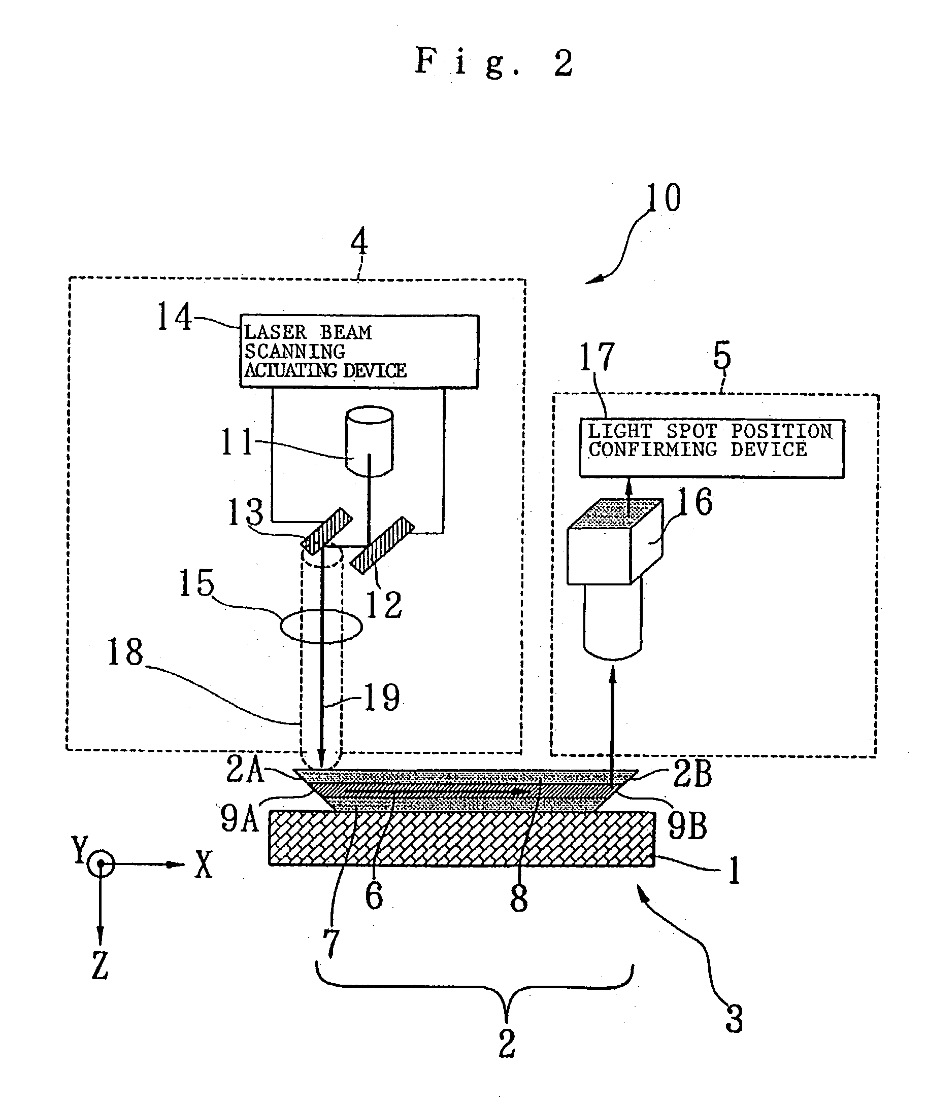
[0028]A method of inspecting an optical waveguide substrate according to a first embodiment of the present invention will be described below with reference to FIGS. 1 through 5.

[0029]As shown in FIG. 2, inspecting apparatus 10 used to carry out a method of inspecting an optical waveguide substrate according to a first embodiment of the present invention comprises laser beam scanning optical system 4 disposed on the side of an end face of optical waveguide substrate 3 (an object to be inspected) which comprises optical waveguide 2 disposed on base substrate 1, and light detecting system 5 disposed on the side of other end face of optical waveguide substrate 3. Optical waveguide 2, which serves as a major component of optical waveguide substrate 3, comprises core layer 6 having a high refractive index and lower and upper cladding layers 7, 8, each having a low refractive index, sandwiching core layer 6 therebetween. End face 2A of optical waveguide 2 has first mirror surface 9A slante...

3rd embodiment

[0054]A method of inspecting an optical waveguide substrate according to a third embodiment of the present invention will be described below with reference to FIGS. 8 and 9. The method of inspecting an optical waveguide substrate according to the third embodiment differs from the method according to the first embodiment in that it inspects an optical waveguide substrate by changing the direction of a laser beam applied to an end face of the optical waveguide.

[0055]As shown in FIG. 8, an inspecting apparatus 30 used to carry out the method according to the third embodiment comprises laser beam scanning optical system 26 disposed on the side of an end face of optical waveguide substrate 3 (an object to be inspected) which comprises optical waveguide 2 disposed on base substrate 1, and light detecting system 5 disposed on the side of other end face of optical waveguide substrate 3. The details of light detecting system 5 are substantially the same as those of light detecting system 5 s...


PUM

PropertyMeasurementUnit
refractive indexaaaaaaaaaa
angleaaaaaaaaaa
spot diameteraaaaaaaaaa

Abstract

There is disclosed a method of inspecting an optical waveguide substrate for optical conduction at an increased inspecting rate and also inspecting an optical waveguide substrate for cross-talk. According to the disclosed method, a laser beam is applied from a laser beam scanning optical system to one end face of an optical waveguide of an optical waveguide substrate which is an object to be inspected, and the laser beam emitted from the other end of the optical waveguide is detected by a CCD camera, which output detected result data. A light spot position confirming device compares the detected result data with stored data.

Description

BACKGROUND OF THE INVENTION[0001]1. Field of the Invention[0002]The present invention relates to a method of inspecting an optical waveguide substrate comprising an optical waveguide disposed on a substrate, and a method of inspecting an optical component mounted on an optical waveguide substrate.[0003]2. Description of the Related Art[0004]Optical communications technologies using light as an information transmitting medium have been in widespread usage. According to the optical communications technologies, an optical waveguide substrate comprising an optical waveguide disposed on a substrate is used for transmitting an optical signal which represents light modulated by an information signal, and the optical signal is transmitted along the optical waveguide substrate. The optical waveguide substrate comprises a core layer having a high refractive index and a cladding layer having a low refractive index, the core layer being surrounded by the cladding layer. An optical signal which ...

Claims


Application Information

Patent Timeline
Patent Type & Authority Patents(United States)
IPC IPC(8): G01N21/00G01M11/00
CPCG01M11/35
Inventor KIKUCHI, HIDEOODA, MIKIOKOUTA, HIKARUKITAJO, SAKAESHIMADA, YUZOMATSUMOTO, YOSHIOTAMABAYASHI, SHINICHI
Owner NEC TOPPAN CIRCUIT SOLUTIONS
Why Eureka
Try Eureka