Semiconductor device

a technology of semiconductors and devices, applied in the direction of semiconductor devices, basic electric elements, electrical appliances, etc., can solve the problems of increasing device pitch and increasing on-resistance, and achieve the effects of high operation speed, reduced switching losses, and high integration

Inactive Publication Date: 2006-09-19
FUJI ELECTRIC HLDG CO LTD
View PDF5 Cites 36 Cited by
  • Summary
  • Abstract
  • Description
  • Claims
  • Application Information

AI Technical Summary

Benefits of technology

[0020]The invention was made in view of the above problems with an object of providing a semiconductor device provided with a trench lateral IGBT (hereinafter referred to as a TL-IGBT) having a small device pitch by which the IGBT can be highly integrated. Moreover, it is also an object of the invention to eliminate the substrate current of the TL-IGBT in a semiconductor device provided with the TL-IGBT, to enable realization of a reduction in switching losses and a high operation speed.
[0021]A further object of the invention to reduce on-resistance in the semiconductor device provided with the TL-IGBT to be less than those in a TLPM and a planar lateral IGBT. In addition, it is an object of the invention to prevent latchup in a semiconductor device in which the TL-IGBTs are integrated together, or to prevent malfunctions due to interaction between transistors in a semiconductor device in which the TL-IGBT and elements such as CMOS devices are integrated together.

Problems solved by technology

Therefore, integration of the TLPM and a CMOS device for controlling the TLPM has a possibility of causing latchup due to interaction between transistors.
Moreover, there also arises a problem that the laterally extended drift region causes an increase in the device pitch, which in turn results in an increase in on-resistance.

Method used


Image

  • Semiconductor device
  • Semiconductor device
  • Semiconductor device

Examples


Embodiment Construction

[0069]In the following, embodiments of the invention will be explained in detail in terms of modes for carrying out the invention, with reference to drawings.

First Mode

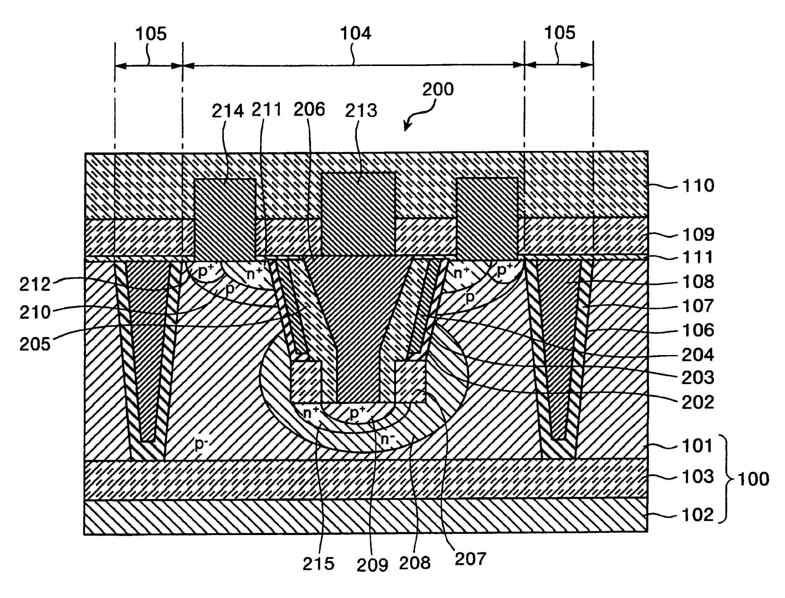
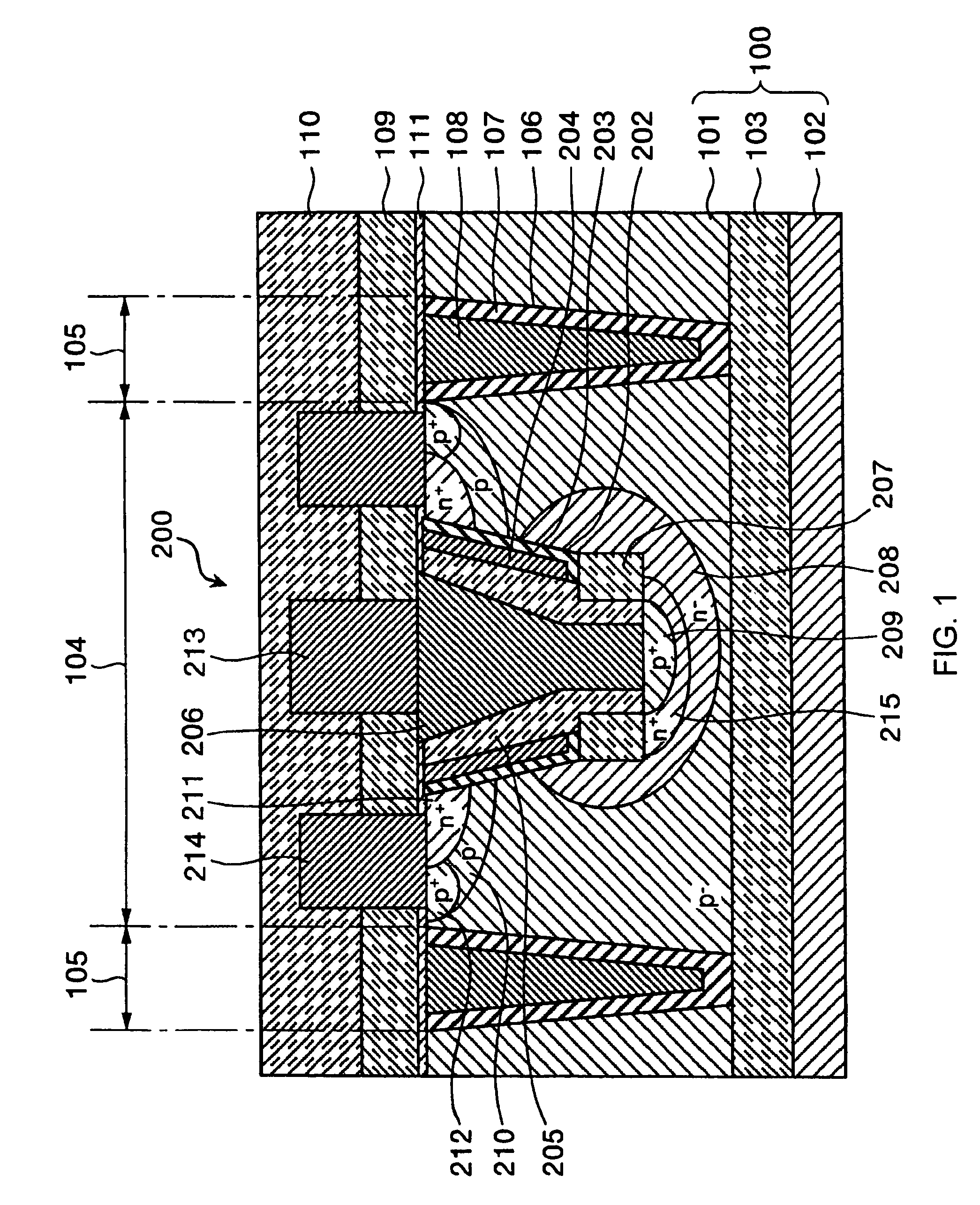
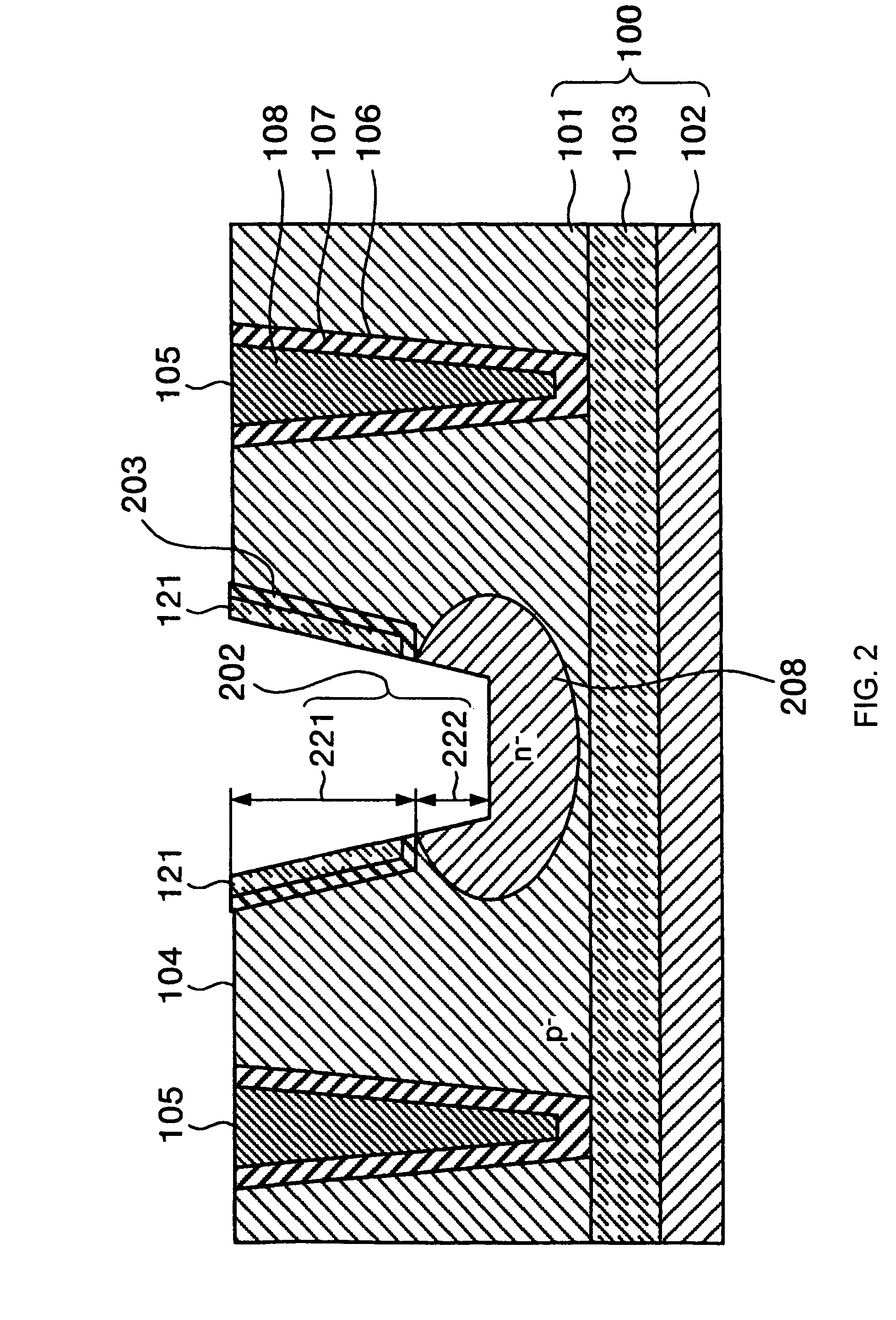
[0070]FIG. 1 is a cross-sectional view showing an arrangement of a semiconductor device according to a first mode for carrying out the invention. The semiconductor device of the first mode is a TL-IGBT provided with a collector contact at the bottom of a trench (hereinafter referred to as a TL-IGBT / C). As shown in FIG. 1, the TL-IGBT / C 200 is formed on an SOI substrate 100 with a structure in which a p−-single-crystal silicon semiconductor layer (hereinafter referred to as a p−-semiconductor layer) 101 is formed on an oxide film 103 provided as an insulator layer on the surface of a semiconductor supporting substrate (hereinafter referred to as a supporting substrate) 102.

[0071]In the p−-semiconductor layer 101, an element-forming region 104 is formed like an island while being isolated by a trench isolation region 10...


PUM


Abstract

A semiconductor structure with device trench and a semiconductor device in the device trench, that enables realization of high integration, lowered on-resistance, reduction in switching losses and a high operation speed in a semiconductor device provided with a lateral IGBT, and that prevents malfunctions such as latchup when IGBTs or an IGBT and CMOS devices are integrated together. The structure includes an SOI substrate having a supporting substrate, an oxide film and a p−-semiconductor layer. An island-like element-forming region is isolated by a trench isolation region from surroundings. The trench isolation region includes an isolation trench with an insulation film on its inner wall. The device trench is formed in the element-forming region. A gate electrode is formed with a gate insulator film in the device trench. A collector region and an emitter region outside are provided respectively on the bottom and the outside of the device trench.

Description

BACKGROUND OF THE INVENTION[0001]1. Field of Invention[0002]The invention relates to a semiconductor device. More particularly, the invention relates to an insulated gate semiconductor device with low on-resistance, used for a high breakdown voltage IC to control a large current, such as an IC for a switching power source. The invention also relates to an IC for driving an automotive power system and to an IC for a plasma display panel driver.[0003]2. Prior Art[0004]In recent years, with the rapid spread of portable information appliances and the development of information technology, power ICs containing power MOSFETs are becoming more important. As for a power IC with a lateral power MOSFET and a control circuit thereof being integrated together, expectations are placed on downsizing, lowered power consumption, increased reliability and reduced cost. This is in contrast to a previous arrangement of a combination of a discrete power MOSFET with control and driving circuits. Thus, o...

Claims


Application Information

Patent Timeline
Patent Type & Authority Patents(United States)
IPC IPC(8): H01L29/739H01L29/78H01L21/762H01L21/77H01L21/84H01L27/12H01L29/417H01L29/423
CPCH01L21/76283H01L21/84H01L27/1203H01L29/7394H01L29/4232H01L29/4238H01L29/41766
Inventor SUGI, AKIOFUJISHIMA, NAOTO
Owner FUJI ELECTRIC HLDG CO LTD
Why Eureka
Try Eureka