Drive circuit of active matrix type organic EL panel and organic EL display device using the same drive circuit

a drive circuit and active matrix technology, applied in the direction of electric digital data processing, instruments, computing, etc., can solve the problems of difficult control of luminance of color display, uneven luminance, and uneven luminance, so as to reduce luminance unevenness, restrict the luminance unevenness of display screen, and reduce luminance unevenness

Active Publication Date: 2006-09-19
ROHM CO LTD
View PDF10 Cites 19 Cited by
  • Summary
  • Abstract
  • Description
  • Claims
  • Application Information

AI Technical Summary

Benefits of technology

[0013]An object of the present invention is to provide a drive circuit of an active matrix type organic EL panel, which is capable of reducing luminance unevenness of a display screen and is particularly suitable for high luminance color display even when the circuit size of pixel circuit is restricted by removing a circuit for compensating for the operating threshold value of drive transistor.
[0014]Another object of the present invention is to provide an organic EL display device, which has a small pixel circuit size and is capable of reducing luminance unevenness of a display screen.
[0018]In the present invention, since the drive currents are regulated by the current regulation circuits of the current drive circuits provided externally of the respective pixel circuits, the control lines for the program control, which is necessary for unifying the operation threshold values of the drive transistors, are unnecessary. Therefore, the numbers of elements as well as wiring lines of each pixel circuit can be reduced correspondingly. Consequently, the size of each pixel circuit can be reduced.
[0020]Therefore, it is possible to regulate drive currents by externally current-driving the organic EL panel by the external drive circuit while restricting each pixel circuit construction of the active type organic EL panel. The regulation is performed by providing the current regulation circuit in each of the plurality of the current drive circuits for driving the pixel circuits located in at least the dispersed positions in the display screen and regulating the drive current values of the pixel circuits by the current regulator circuits in such a way that luminance unevenness becomes unconscious. Thus, it is possible to restrict luminance unevenness of the display screen regardless of variation of the operating threshold value of the drive transistors of the pixel circuits. It is, of course, possible to further reduce the luminance unevenness by providing the current drive circuit having current value regulation circuit for ever data line or column terminal pin.
[0021]As a result, it is possible to restrict the circuit size of each pixel circuit by removing the circuit for compensating for the operating threshold value of the drive transistor and to reduce the luminance unevenness of the display screen.

Problems solved by technology

Known problems of such organic EL display device are that, since, when it is driven by voltage as in a liquid crystal display device, luminance variation thereof becomes substantial and that, since there is difference in sensitivity of organic EL element between R (red), G (green) and B (blue), a control of luminance of a color display becomes difficult.
In such active matrix type organic EL display device, luminance unevenness tends to occur due to variation of operating threshold value of the drive transistor in each of the pixel circuits.
Since it is difficult to make the operating thresholds of the drive transistors of the respective pixel circuit uniform during a fabrication process of the display device, it has been considered to restrict the luminance unevenness by controlling the voltages of the capacitors of the respective pixel circuits.
Therefore, the control itself becomes difficult.

Method used


Image

  • Drive circuit of active matrix type organic EL panel and organic EL display device using the same drive circuit
  • Drive circuit of active matrix type organic EL panel and organic EL display device using the same drive circuit
  • Drive circuit of active matrix type organic EL panel and organic EL display device using the same drive circuit

Examples


Embodiment Construction

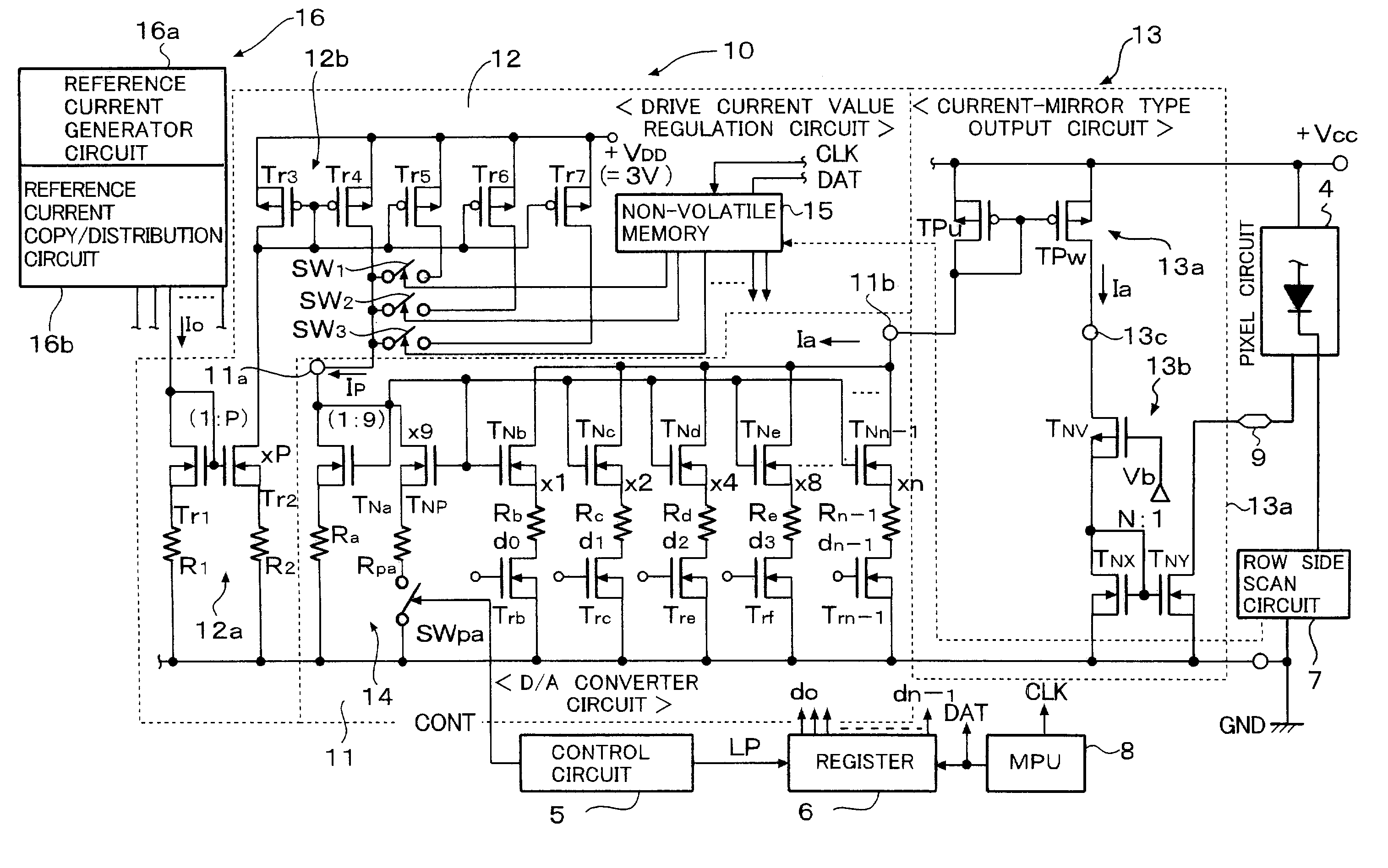
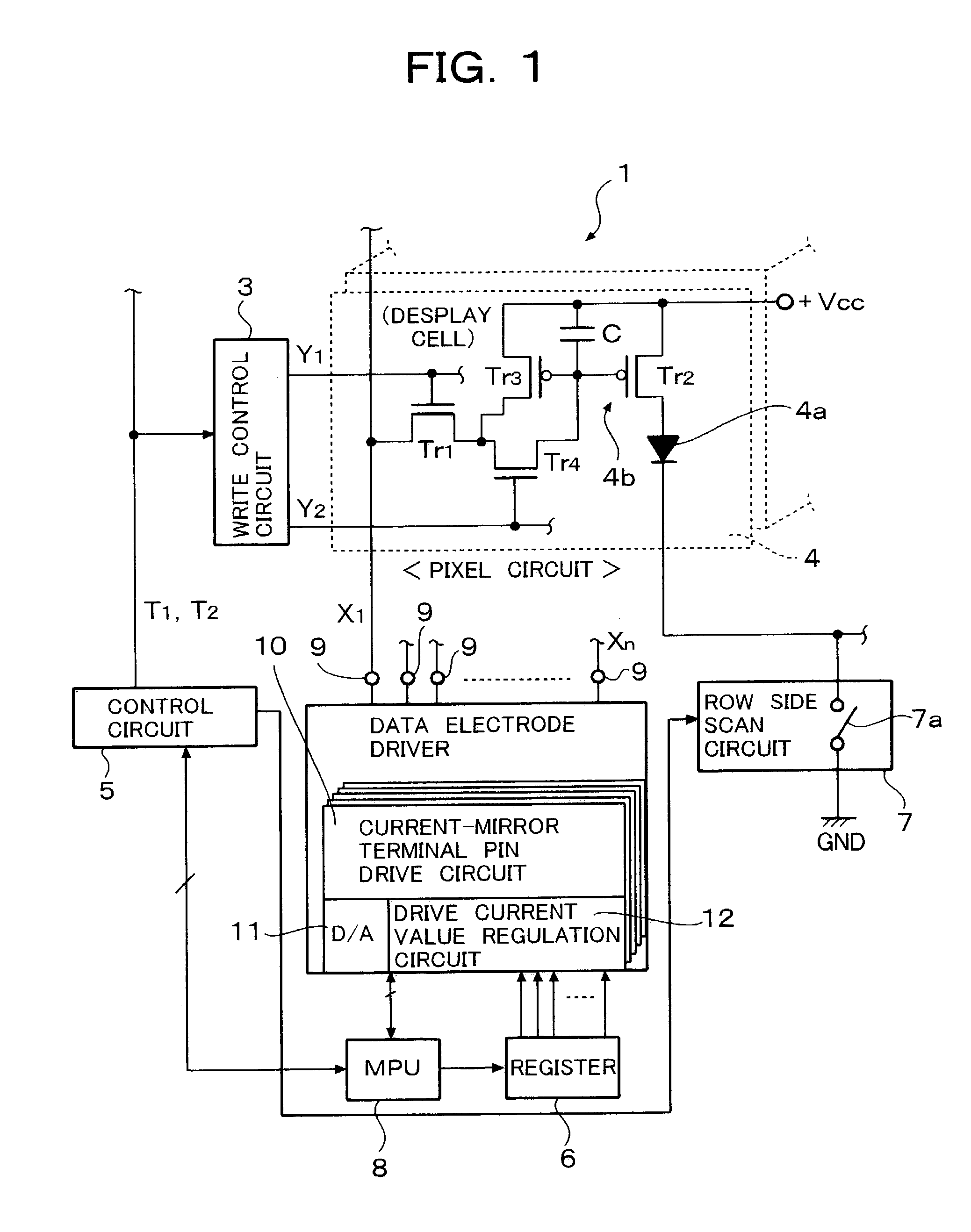
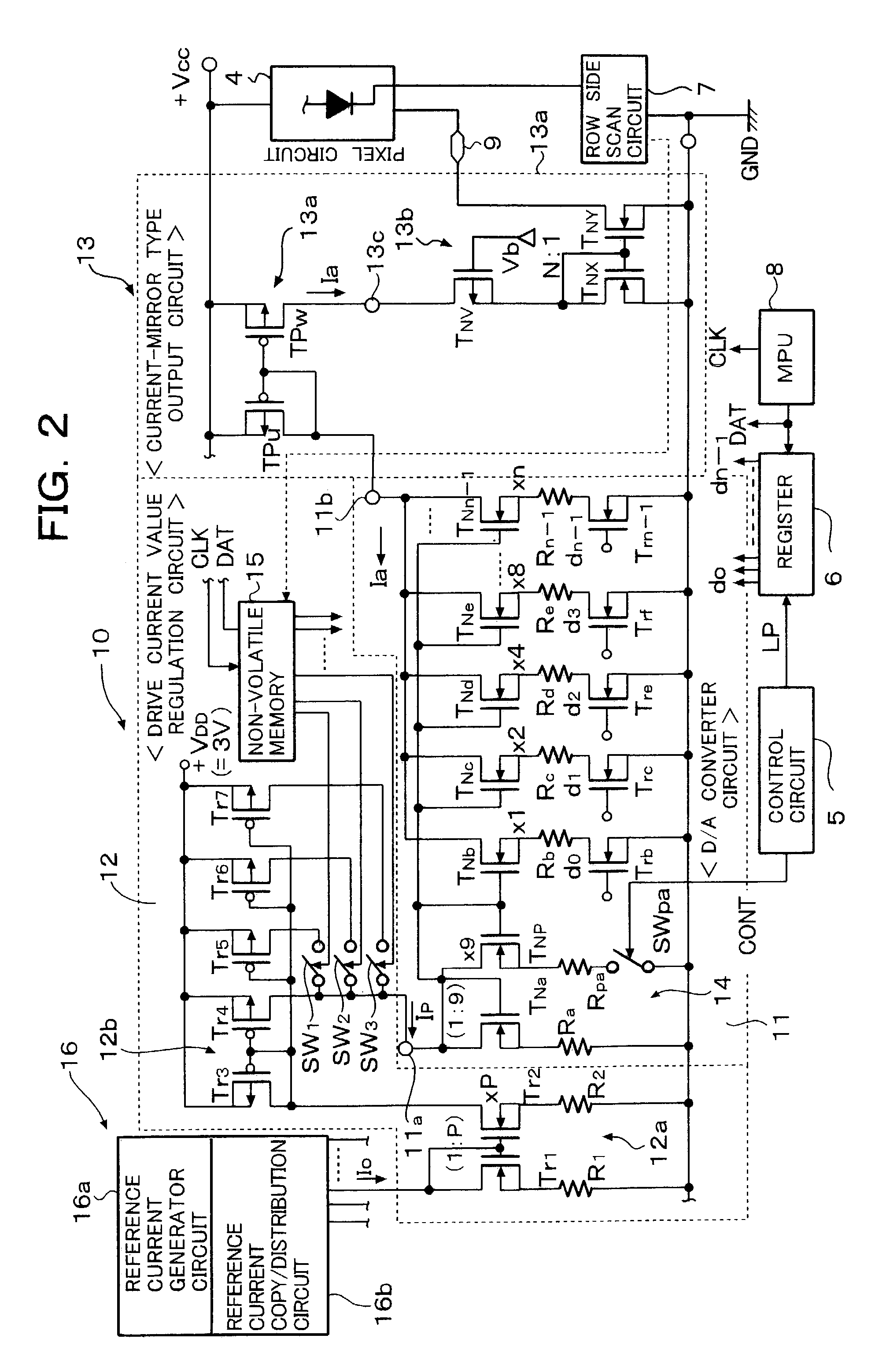
[0027]FIG. 1 is a block circuit diagram of an active matrix type organic EL display device 1. The active matrix type organic EL display device 1 includes a data electrode driver 2, a write control circuit 3, a pixel circuit 4, a control circuit 5, a register 6, a row side scan circuit 7 and an MPU 8, etc. Incidentally, the pixel circuit 4 is provided at every cross point of X and Y matrix lines and only one pixel circuit is shown in FIG. 1 as an representative of the pixel circuits.

[0028]The data electrode driver 2 is a column driver of an organic EL element drive circuit in a horizontal scan direction and includes a plurality of current-mirror terminal pin drive circuits (referred to as “current drive circuits”, hereinafter) 10 provided correspondingly to respective data lines (or column terminal pins). An output pin 9 of each current-mirror output stage circuit 13 (FIG. 2) is connected to one of the data lines (X1, . . . , Xn) of the X and Y matrix lines (data lines and scan lines...


PUM


Abstract

A drive current value is regulated by a current value regulator circuit of a current drive circuit provided externally of each pixel circuit, so that control lines for a program control provided in order to unify operating threshold values of drive transistors becomes unnecessary. Therefore, the number of transistors of each pixel circuit can be reduced and the circuit size of each pixel circuit can be reduced thereby.

Description

BACKGROUND OF THE INVENTION[0001]1. Field of the Invention[0002]The present invention relates to a drive circuit of an active matrix type organic EL panel and an organic EL display device using the drive circuit and, in particular, the present invention relates to an active matrix type organic EL display device, which can reduce luminance unevenness of a display screen of a portable telephone set or PHS, etc., even when the size of pixel circuit is restricted by removing a circuit for compensating for an operating threshold value of drive transistors and is suitable for high luminance color display.[0003]2. Description of the Prior Art[0004]It has been known that an organic EL display device, which realizes a high luminance display by spontaneous light emission, is suitable for a display on a small display screen and the organic EL display device has been attracting public attention as the next generation display device to be mounted on a portable telephone set, a PHS, a DVD player ...

Claims


Application Information

Patent Timeline
Patent Type & Authority Patents(United States)
IPC IPC(8): G09G3/30G09G3/32
CPCG09G3/3241G09G3/3283G09G2320/0233G09G2310/0251G09G2310/027G09G2300/0842G09G3/30
Inventor ABE, SHINICHIFUJISAWA, MASANORI
Owner ROHM CO LTD
Why Eureka
Try Eureka