
Non-volatile memory configuration scheme for volatile-memory-based programmable circuits in an FPGA

a programmable circuit and volatile memory technology, applied in the field of integrated circuit technology, can solve the problems of not being able to efficiently route one signal, not having enough physical space or architectural bandwidth, and compromising the effective bandwidth of dynamic signals. the number of such conductors becomes unreasonably larg

Active Publication Date: 2006-09-26
MICROSEMI SOC
View PDF6 Cites 33 Cited by
  • Summary
  • Abstract
  • Description
  • Claims
  • Application Information

AI Technical Summary

Problems solved by technology

In addition, as the control requirements proliferate, there may not be enough physical room or architectural bandwidth to efficiently route one signal per control bit to the external element without compromising the effective bandwidth of the dynamic signals.
At some point, the number of such conductors becomes unreasonably large and can become a critical design issue.

Method used


Image

  • Non-volatile memory configuration scheme for volatile-memory-based programmable circuits in an FPGA
  • Non-volatile memory configuration scheme for volatile-memory-based programmable circuits in an FPGA
  • Non-volatile memory configuration scheme for volatile-memory-based programmable circuits in an FPGA

Examples


Embodiment Construction

[0015]Those of ordinary skill in the art will realize that the following description of the present invention is illustrative only and not in any way limiting. Other embodiments of the invention will readily suggest themselves to such skilled persons.

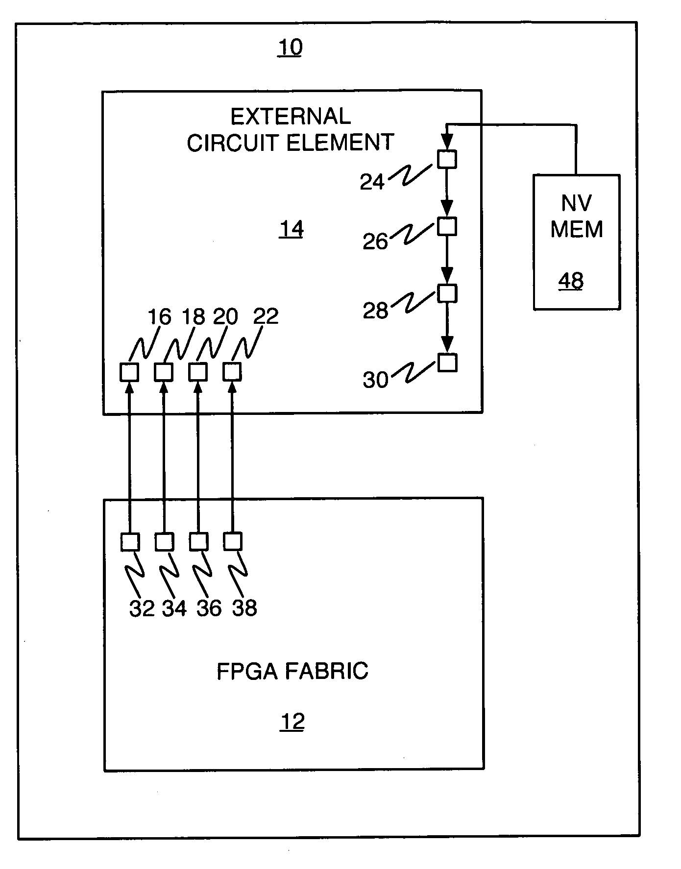
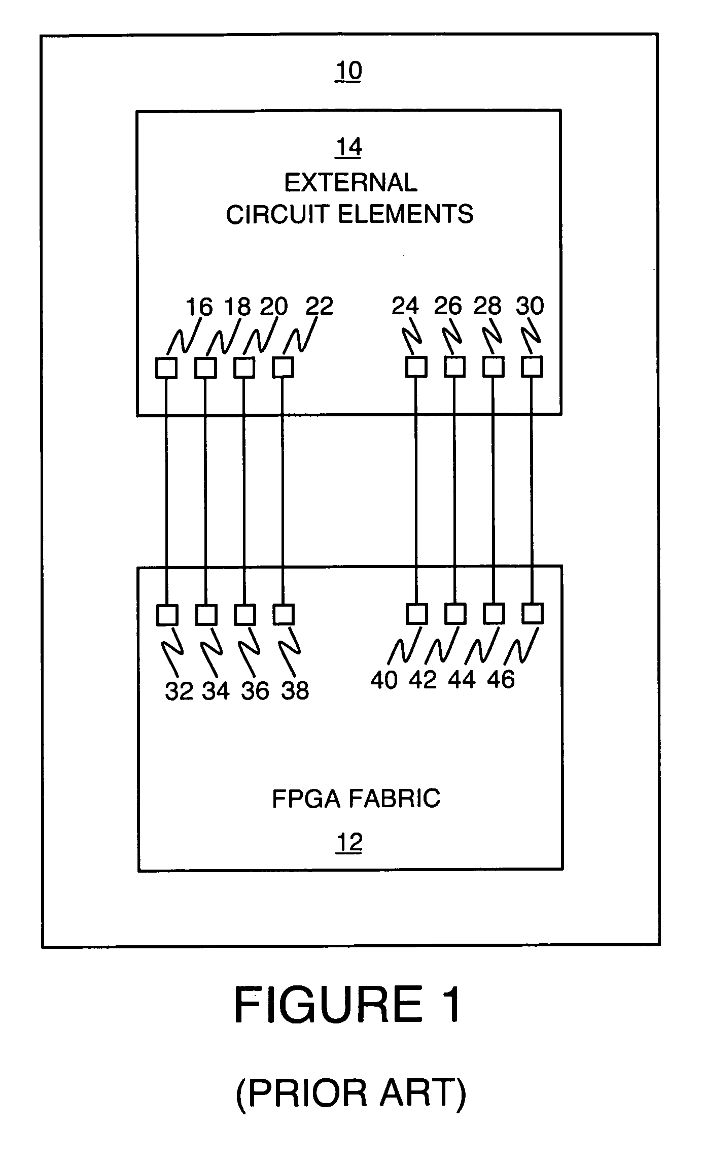
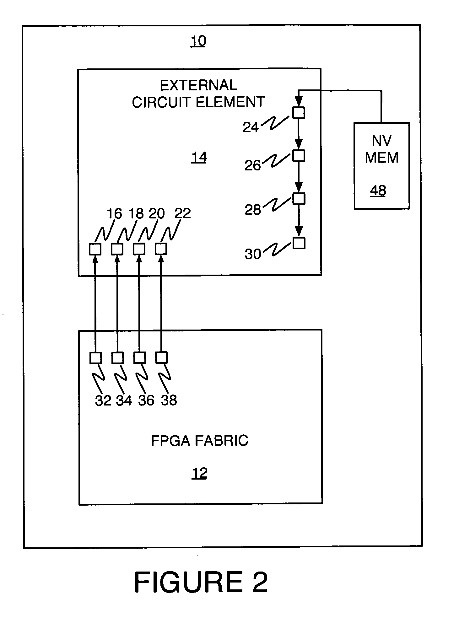
[0016]Referring now to FIG. 2, a block diagram presents an illustrative arrangement for configuring circuit elements external to an FPGA fabric in an integrated circuit according to the principles of the present invention. As in the circuit arrangement of FIG. 1, the arrangement of FIG. 2 shows an integrated circuit 10 including an FPGA fabric 12 and a group of external configurable circuit elements 14. As in FIG. 1, representative ones of such configurable circuit elements are represented by small squares 16, 18, 20, 22, 24, 26, 28, and 30.

[0017]The configurable circuit elements 16, 18, 20, and 22 are shown in FIG. 2 as being controlled, respectively, by configuration bits 32, 34, 36, and 38, distributed throughout the FPGA fabric 12. ...


PUM


Abstract

A non-volatile memory configuration scheme is disclosed for volatile-memory-based programmable circuits in a programmable integrated circuit that includes an FPGA fabric, a plurality of first configurable circuit elements external to the FPGA fabric, and a plurality of second configurable circuit elements external to the FPGA fabric. A plurality of distributed configuration non-volatile memory cells is disposed in the FPGA, each one of the distributed configuration non-volatile memory cells coupled to a different one of the plurality of first configurable circuit elements. A non-volatile memory array stores configuration information for the second configurable circuit elements. A plurality of register cells is disposed with the second configurable circuit elements and is coupleable to the non-volatile memory array, each one of the register cells coupled to a different one of the plurality of second configurable circuit elements.

Description

BACKGROUND[0001]The present invention relates to integrated circuit technology. More particularly, the present invention relates to programmable logic circuits, such as FPGAs, and particularly flash-based programmable logic circuits. The present invention addresses how to efficiently provide static control signals to circuit elements external to the FPGA fabric without compromising the bandwidth of the dynamic signal path.[0002]An FPGA integrated circuit includes many circuit elements in addition to the FPGA fabric that require bits to control their functionality. A typical example is a general purpose I / O cell which typically has three dynamic signals (i.e., input, output, enable) that must be capable of being driven by a net from and to the FPGA.[0003]Accompanying these signals are usually several control signals (which may number ten or more) that typically do not need connectivity to a net but need to be statically set. Such signals include those to configure the I / O standard be...

Claims


Application Information

Patent Timeline
Patent Type & Authority Patents(United States)
IPC IPC(8): H03K19/173
CPCH03K19/17756H03K19/17776H03K19/17772H03K19/17758
Inventor SPEERS, THEODORE
Owner MICROSEMI SOC
Learn More