

Image display having internal wiring with multi-layer structure and manufacturing method thereof having particular wiring connection
a technology of internal wiring and multi-layer structure, applied in the field of image displays, can solve the problems of increasing the resistance value of internal wiring, affecting the display properties, and enlarge the external size of the display panel
- Summary
- Abstract
- Description
- Claims
- Application Information
AI Technical Summary
Benefits of technology
Problems solved by technology
Method used
Image

Examples
embodiment 1
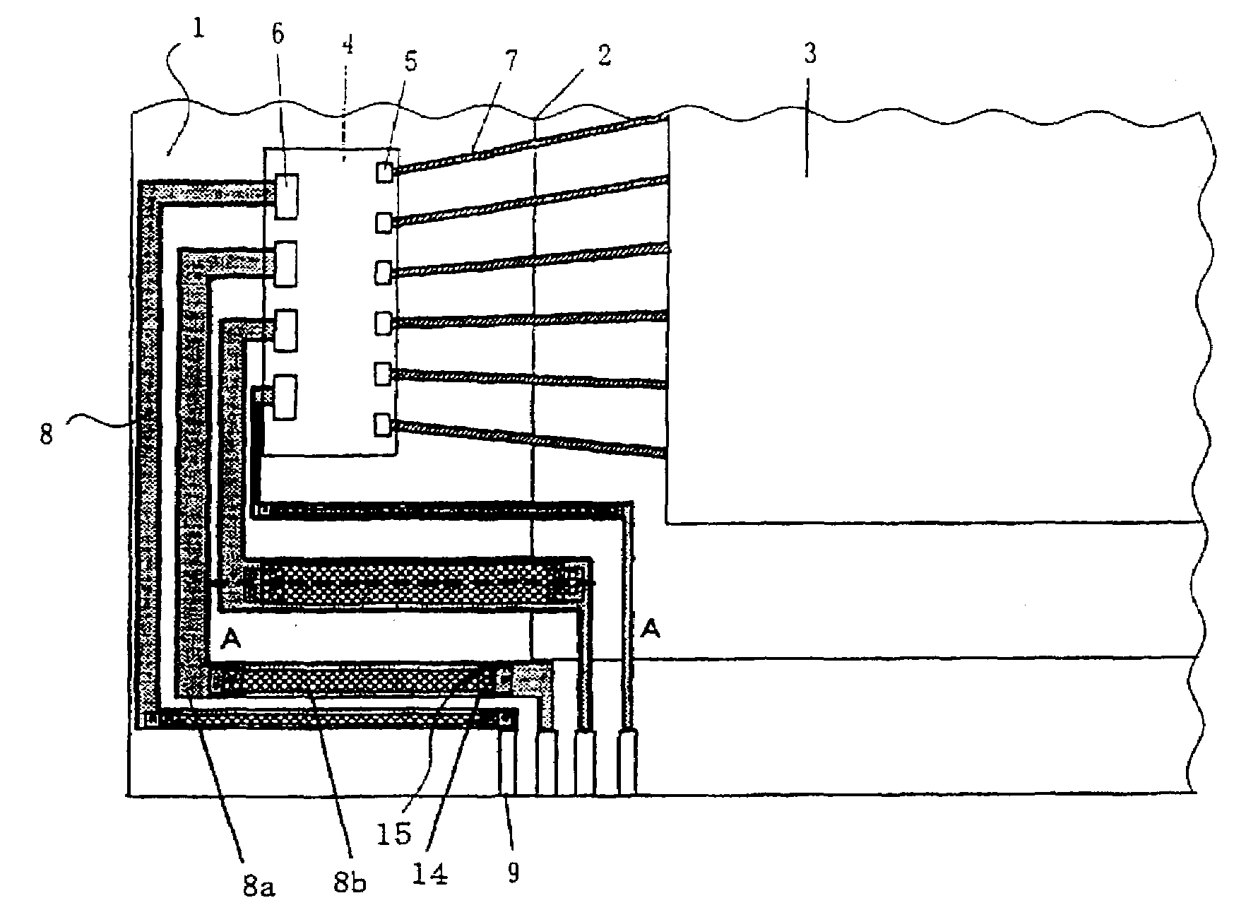
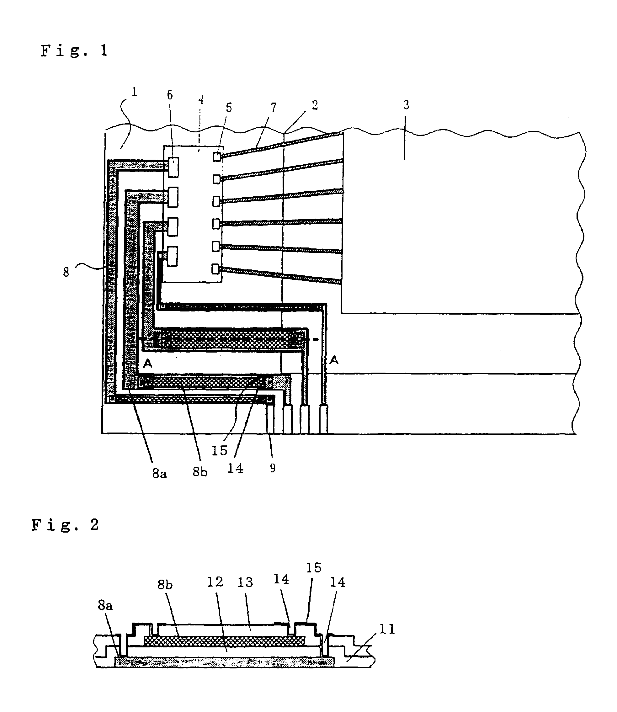
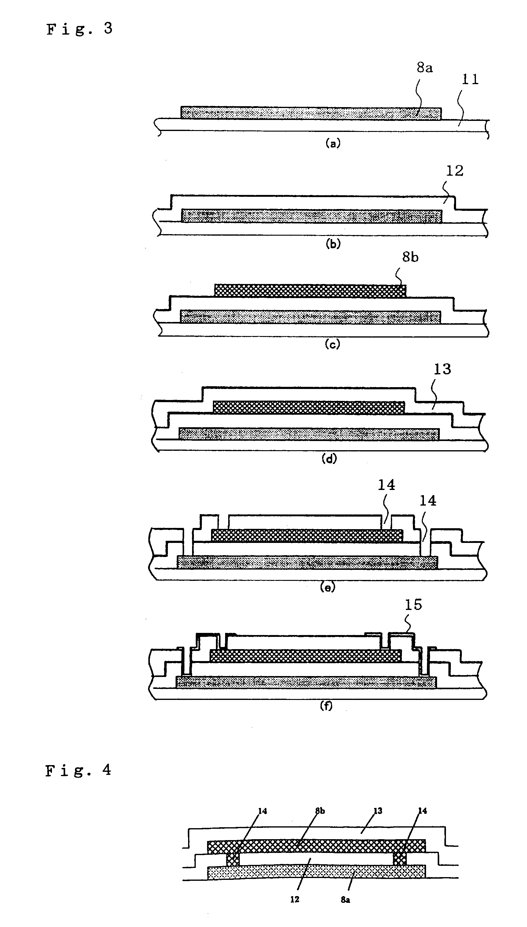
[0041]An image display according to an embodiment of the invention is hereinafter described with reference to the drawings. FIG. 1 is a plan view showing a part of the image display (liquid crystal display in this embodiment) according to Embodiment 1 of the invention, and FIG. 2 is a sectional view taken along the line A—A in FIG. 1. FIGS. 3(a) to (f) are sectional views each showing a manufacturing process taken along the line A—A in FIG. 1.
[0042]In the drawings, reference numeral 1 is a first substrate (TFT array substrate in this embodiment) forming the image display (the liquid crystal display in this embodiment). Numeral 2 is a second substrate (opposed substrate in this embodiment) opposed to the TFT array substrate 1, and a liquid crystal material is held between the TFT array substrate 1 and the opposed substrate 2. Numeral 3 is a display area of the image display, numeral 4 is a COG-packaged driving IC mounted in the packaging area on the TFT array substrate 1. Numeral 5 i...
embodiment 2
[0057]FIG. 5 is a plan view showing a part of an image display (liquid crystal display in this embodiment) according to Embodiment 2 of the invention. In the drawing, numeral 21 is internal wiring for inputting a power supply, and numeral 22 is internal wiring for inputting a signal.
[0058]Other reference numerals, features, and manufacturing process are the same as those in the foregoing Embodiment 1, and further explanation of them is omitted herein.
[0059]In the foregoing Embodiment 1, the whole internal wiring 8 for inputting a signal and a power supply to the driving IC 4 is formed into two layers. In this embodiment, however, as shown in FIG. 5, the internal wiring 21 for inputting a power supply having a resistance of a small allowance value is composed of two layers, and the internal wiring 22 for inputting a signal having a resistance of a relatively large allowance value is composed of one layer. As a result, it is possible to obtain the same advantage as obtained in Embodim...
embodiment 3
[0060]FIG. 6 is a plan view showing a part of an image display (liquid crystal display in this embodiment) according to Embodiment 3 of the invention.
[0061]The reference numerals in the drawing, features, and manufacturing process are the same as those in the foregoing Embodiment 1, and further explanation of them is omitted herein.
[0062]In the liquid crystal display according to this Embodiment 3, the internal wiring 8 is composed of one layer, i.e., either the first layer internal wiring 8a or the second layer internal wiring 8b in the area where the opposed substrate 2 is laid on the packaging area of the TFT array substrate 1. On the other hand, the internal wiring 8 is composed of two layers, i.e., the first layer internal wiring 8a and the second layer internal wiring 8b in an area where the opposed substrate 2 is not laid on the TFT array substrate 1.
[0063]Thus, in the case where the internal wiring 8 composed of two layers is formed in the area where the TFT array substrate ...
PUM
| Property | Measurement | Unit |
|---|---|---|
| power | aaaaa | aaaaa |
| conductive | aaaaa | aaaaa |
| insulating | aaaaa | aaaaa |
Abstract
Description
Claims
Application Information