

Array substrate and method of manufacturing the same, and liquid crystal display screen
a technology of array substrate and liquid crystal display screen, which is applied in the field of array substrate and method of manufacturing the same, can solve the problems of increased total impact of common electrode, inability to maintain a stable level, and difference in display color, so as to reduce resistance value, reduce resistance value, and reduce resistance value
- Summary
- Abstract
- Description
- Claims
- Application Information
AI Technical Summary
Benefits of technology
Problems solved by technology
Method used
Image

Examples
first embodiment
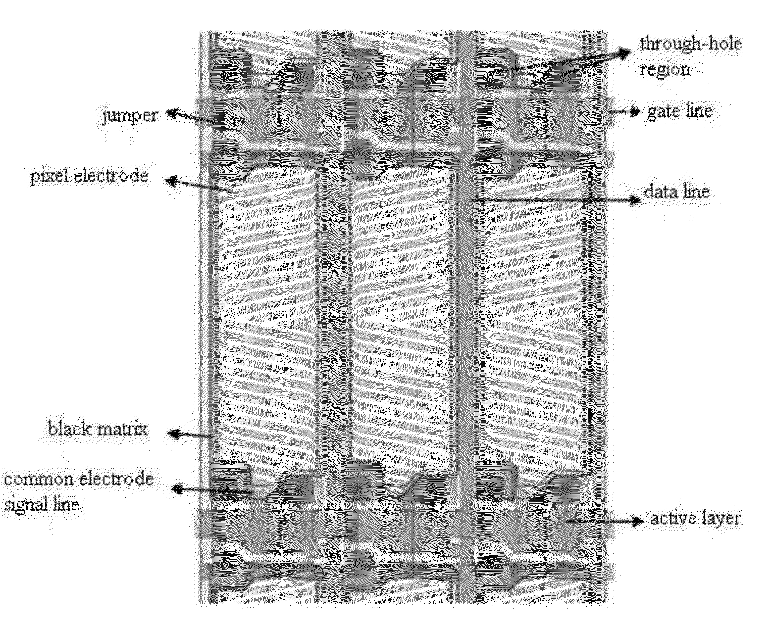
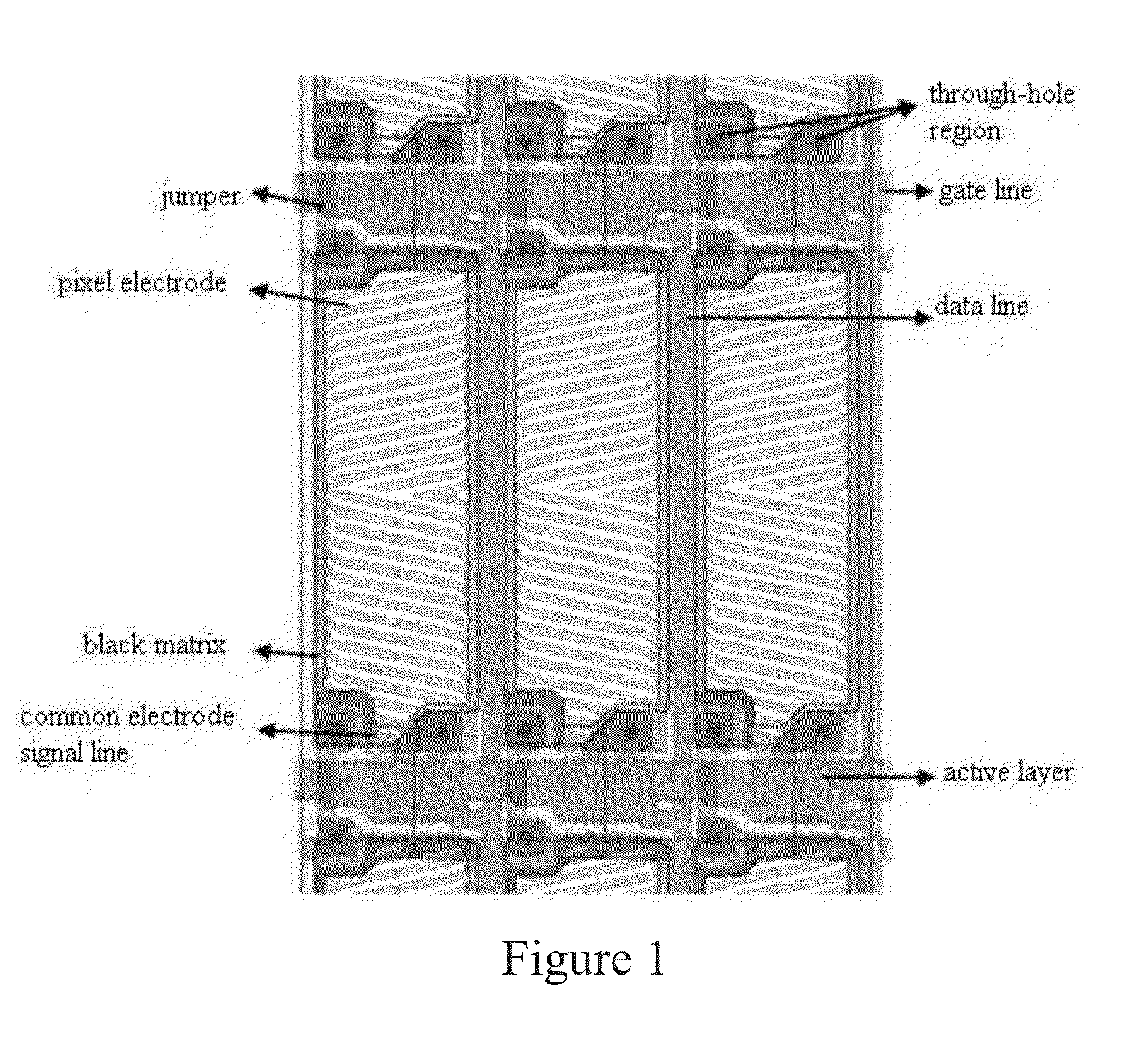
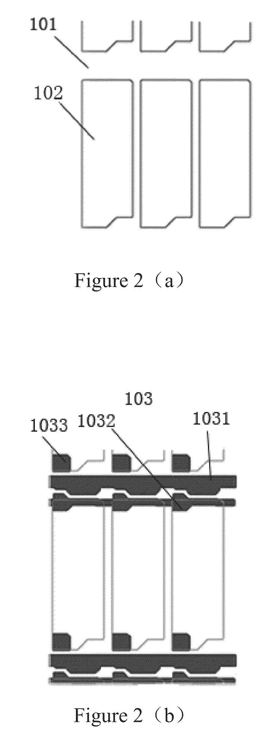
[0038]FIG. 3(a)˜FIG. 3(e) show plan views of a structure of, and flowcharts of processes of manufacturing, an array substrate in the present invention. As shown in FIG. 3(a)˜FIG. 3(e), the array substrate, in its cross-sectional configuration, comprises a substrate 201, common electrodes 202, a gate layer 203, a layer of active material and source-drain electrodes 204, a passivation layer 205 and a pixel electrode layer 206. As shown in FIG. 3(a), the common electrodes 202 are arranged on the substrate 201 in an array manner. As shown in FIG. 3(b), the gate layer 203 covers on the substrate 201 formed with the common electrodes 202, and as can be seen from FIG. 3(b), the gate layer 203 is etched to form gate lines 2031, common electrode signal lines 2032 above the common electrodes, and first through-hole regions 2033 below the common electrode, each common electrode signal line 2032 is used to connect the common electrodes for the same row of pixel units. A common electrode connect...
second embodiment
[0065]FIG. 6 shows a method of manufacturing the array substrate provided in the present invention. As shown in FIGS. 4 and 6, the method comprises steps of:
[0066]depositing a common electrode layer on a substrate 201, and etching the common electrode layer to form a plurality of strip common electrodes 202 arranged in an array;
[0067]depositing a gate layer 203 on the substrate 201 formed with the common electrodes 202, and etching the gate layer 203 to form a gate line 2031 between upper and lower rows of pixel units, a common electrode signal line 2032 located in a horizontal direction above the common electrode 202 for a row of pixel units, a first through-hole region 2033 located leftward below each common electrode 202, and a common electrode connection line 2034 between the common electrode signal line 2032 located above one common electrode 202 and the first through-hole region 2033 located leftward below the same one common electrode 202; wherein the common electrode signal ...
PUM
| Property | Measurement | Unit |
|---|---|---|
| conductive | aaaaa | aaaaa |
| resistivity | aaaaa | aaaaa |
| electric field | aaaaa | aaaaa |
Abstract
Description
Claims
Application Information