Non-volatile memory device and data storing method

a non-volatile memory and data storage technology, applied in the direction of memory adressing/allocation/relocation, digital storage, instruments, etc., can solve the problems of large overhead and long total write time, and achieve the effect of reducing the overhead of write data transfer, reducing the time required for writing data, and facilitating the next data

Inactive Publication Date: 2006-10-03
RENESAS ELECTRONICS CORP
View PDF18 Cites 11 Cited by
  • Summary
  • Abstract
  • Description
  • Claims
  • Application Information

AI Technical Summary

Benefits of technology

[0007]It is an object of the present invention to provide a technology that reduces the write-data transfer overhead of a card storage device containing a non-volatile memory and a buffer memory to reduce the data write time.
[0010]According to the above aspect, data is transferred from the host CPU to the buffer memory concurrently with the data transfer from the buffer memory to the non-volatile memory. This method reduces the write data transfer overhead and greatly reduces the time required for writing data.
[0011]According to another aspect of the present invention, the card storage device further comprises a status register or a status flag indicating a completion / incompletion of the data transfer from the buffer memory to the non-volatile memory, wherein the status of the status register or the status flag are controlled by the controller. This configuration allows the host CPU to reference the status register or the status flag and to determine easily whether the next data may be transferred from the host CPU to the buffer memory.
[0012]According to another aspect of the present invention, the card storage device further comprises a first register containing information on a bank into which data is being entered from the external unit; and a second register containing information on a bank from which data is being transferred from the buffer memory to the non-volatile memory, wherein the controller judges the completion / incompletion of the data transfer to or from each bank, based on the bank information in the first register and the second register, to control the status register or the status flag. Alternatively, the card storage device further comprises a flag, for each bank, indicating whether or not the corresponding bank has data to be transferred to the non-volatile memory, wherein the controller judges the completion / incompletion of the data transfer to or from each bank, based on the flag status, to control the status register or the status flag. This configuration makes it easy to concurrently control the transfer of data from the buffer memory to the non-volatile memory and the transfer of data from the host CPU to the buffer memory.

Problems solved by technology

However, the problem with this method is that the overhead is large and that total write time is long because, for period T4 during which data is written into the non-volatile memory, data transfer to the buffer memory is suspended and the host CPU is put in the wait state and because the write operation of the non-volatile memory is also put in the wait state for the period during which the next data is transferred from the host CPU to the buffer memory.

Method used


Image

  • Non-volatile memory device and data storing method
  • Non-volatile memory device and data storing method
  • Non-volatile memory device and data storing method

Examples


first embodiment

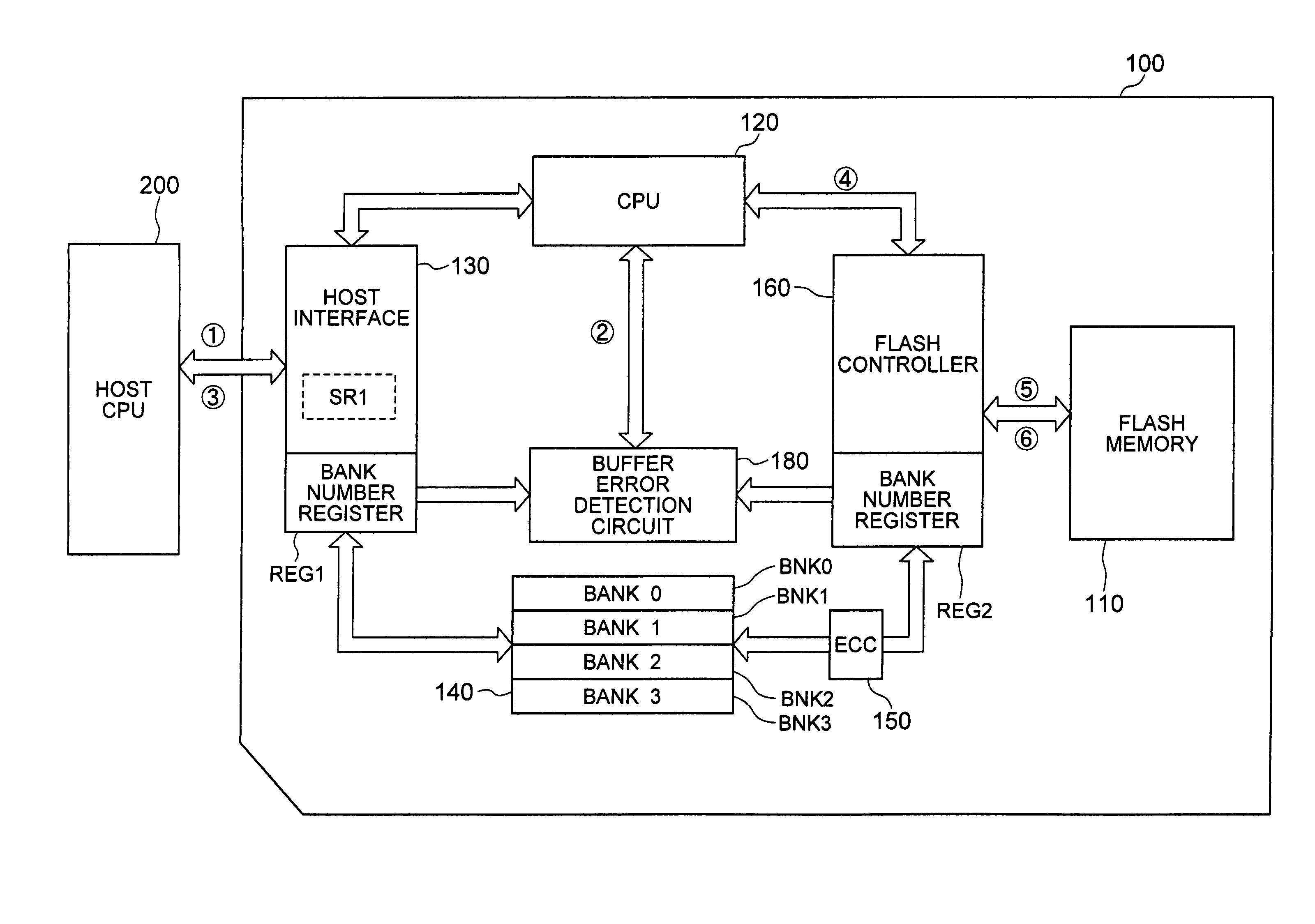
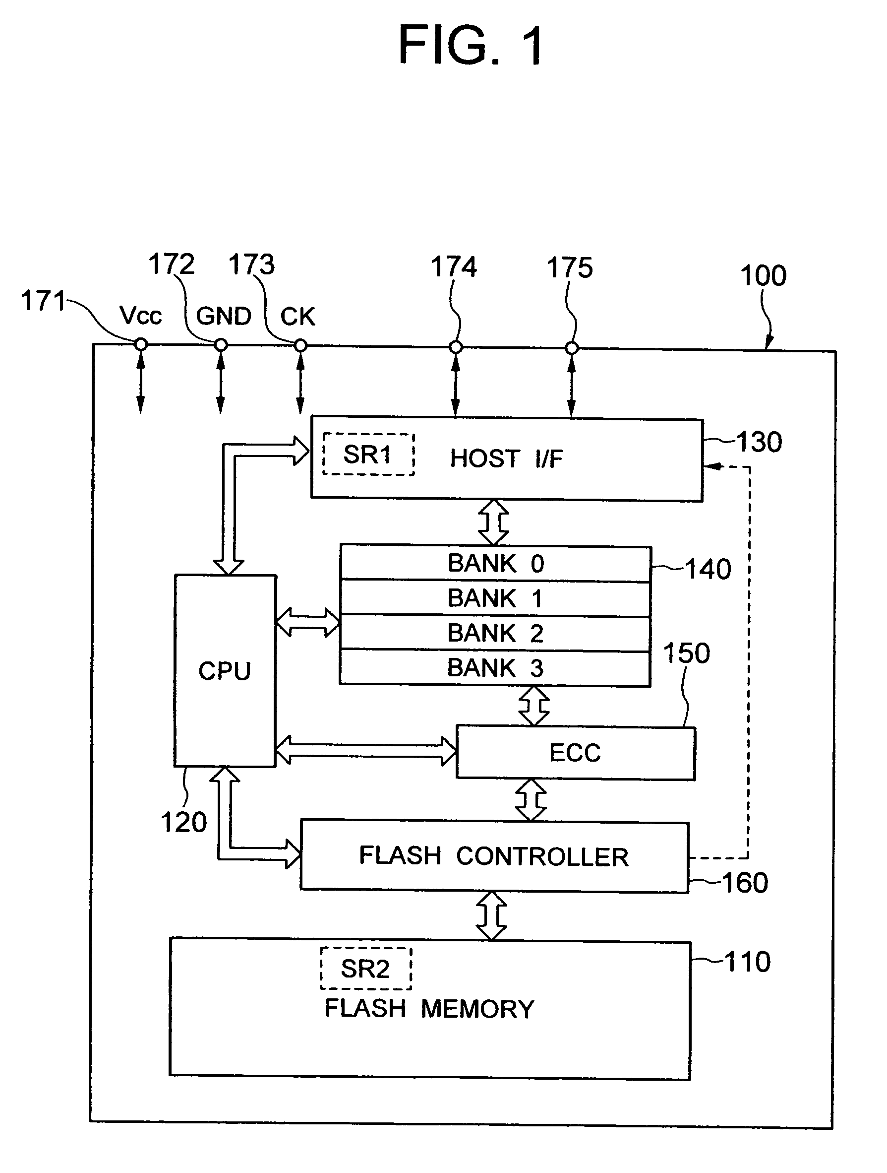
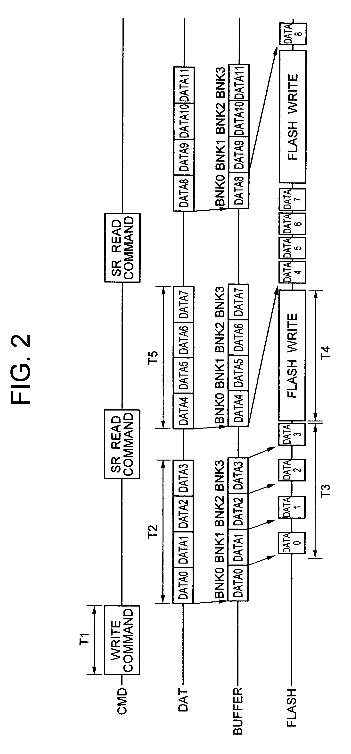
[0040]the write data transfer method that is used when the present invention is applied to the memory card with the configuration described above will be described with reference to the timing diagram in FIG. 2. In the description below, the buffer memory 140 is assumed to include four banks, BNK0–BNK3, each with the capacity of 512 bytes.

[0041]In the first embodiment, when data is written in the memory card, a data transfer command and a write address are first sent from an external host CPU to the external terminal 174 of the memory card (period T1). Then, write data is transferred from the host CPU to the external terminal 175 of the memory card. The transferred data is stored sequentially into banks BNK0–BNK3 of the buffer memory 140 via the interface 130 (period T2). The transmission of the command and the address and the transfer of write data described above are performed serially.

[0042]Concurrently with the transfer of write data to the buffer memory 140 described above, wri...

third embodiment

[0060]the write data transfer method for use on the memory card according to the present invention will be described with reference to the timing diagram in FIG. 6.

[0061]The transfer method in the third embodiment is similar to that in the second embodiment. That is, after data DATA0–DATA3 has been transferred to all banks BNK0–BNK43 of the buffer memory 140, data, DATA4–DATA7, to be written into the next sector is immediately transferred without checking if data has been transferred from the buffer memory 140 to the flash memory 110. The difference from the transfer method in the second embodiment is that a buffer error occurs when an attempt is made to transfer the next data if all banks contain data not yet transferred as shown in the buffer memory status diagram at the bottom of FIG. 6 (timing t2). In the buffer memory status diagram at the bottom of FIG. 6, a shaded bank indicates that data from the host CPU is stored but the data is not yet transferred to the flash memory.

[006...


PUM


Abstract

In a card storage device containing a non-volatile memory and a buffer memory, the buffer memory includes a plurality of banks. Data is transferred sequentially from a host CPU to the banks of the buffer memory, data is transferred to the non-volatile memory from a bank that becomes full, a write operation is started when one unit of data to be written into the non-volatile memory at a time has been transferred and, without waiting for the data to be written, the next write data is transferred from the host CPU to a bank from which write data has been transferred.

Description

CROSS-REFERENCE TO RELATED APPLICATION[0001]This application is a division of application Ser. No. 10 / 082,310 filed Feb. 26, 2002 now U.S. Pat. No. 6,731,537.BACKGROUND OF THE INVENTION[0002]The present invention relates to a technology that may be applied to a non-volatile storage device, for example, to a technology that may be applied to a non-volatile semiconductor memory such as a flash memory or a card storage device, such as a multimedia card or a smart media memory card, that contains such a non-volatile semiconductor memory.[0003]Recently, a card storage device, called a memory card containing a non-volatile memory, such as a flash memory, that retains its storage data even after the power has been switched off, is widely used as a data storage medium for portable electronic apparatus such as a digital camera.[0004]Unlike a volatile memory such as a RAM, a non-volatile memory requires a longer write time. To solve this problem, some memory cards that contain a non-volatile ...

Claims


Application Information

Patent Timeline
Patent Type & Authority Patents(United States)
IPC IPC(8): G11C14/00G06F13/00G11C16/04G11C7/10G11C8/00G06F12/00G06F12/06G11C16/02G06K19/07G11C16/10
CPCG11C16/10G11C2207/229
Inventor KANAMORI, MOTOKITAMURA, TAKAYUKIKOZAKAI, KENJISHIKATA, ATSUSHIASARI, SHINSUKE
Owner RENESAS ELECTRONICS CORP
Why Eureka
Try Eureka