LDMOS transistor

a transistor and transistor structure technology, applied in the field of ldmos transistor structure, can solve the problems of limited high frequency performance of ldmos transistors, needing grounding of sources, and further limiting the high frequency performance of devices

Active Publication Date: 2006-10-10
INFINEON TECH AG
View PDF12 Cites 35 Cited by
  • Summary
  • Abstract
  • Description
  • Claims
  • Application Information

AI Technical Summary

Benefits of technology

[0043]Other technical advantages of the present disclosure will be readily apparent to one skilled in the art from the following figures, descriptions, and claims. Various embodiments of the present application obtain only a subset of the advantages set forth. No one advantage is critical to the embodiments.

Problems solved by technology

LDMOS transistors are, however, limited in their high frequency performance due to the feedback capacitance Cdg between the gate and the drain. FIG. 1 shows one type of an LDMOS transistor as known in the art.
Furthermore, grounding of the source is needed.
This type of connection generates a considerable amount of source resistance which further limits the device's high frequency performance.

Method used


Image

  • LDMOS transistor
  • LDMOS transistor
  • LDMOS transistor

Examples


Embodiment Construction

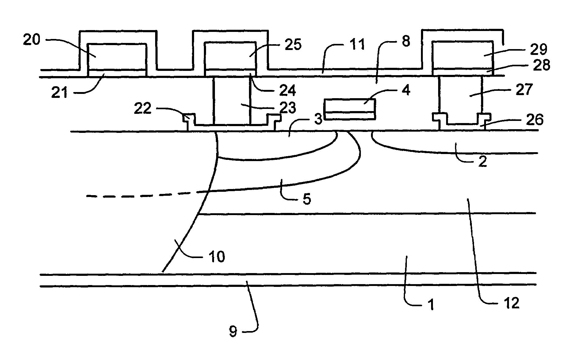
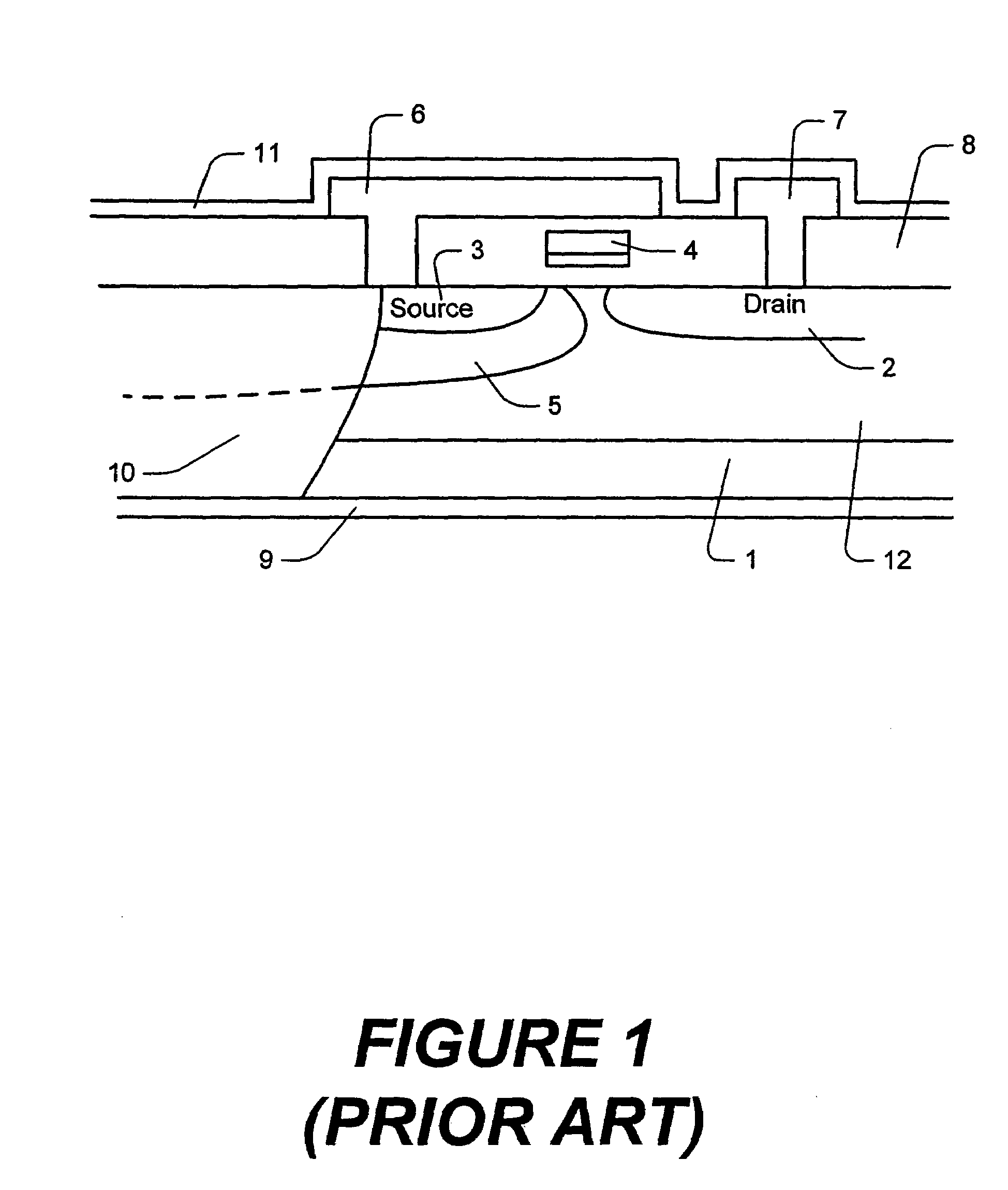
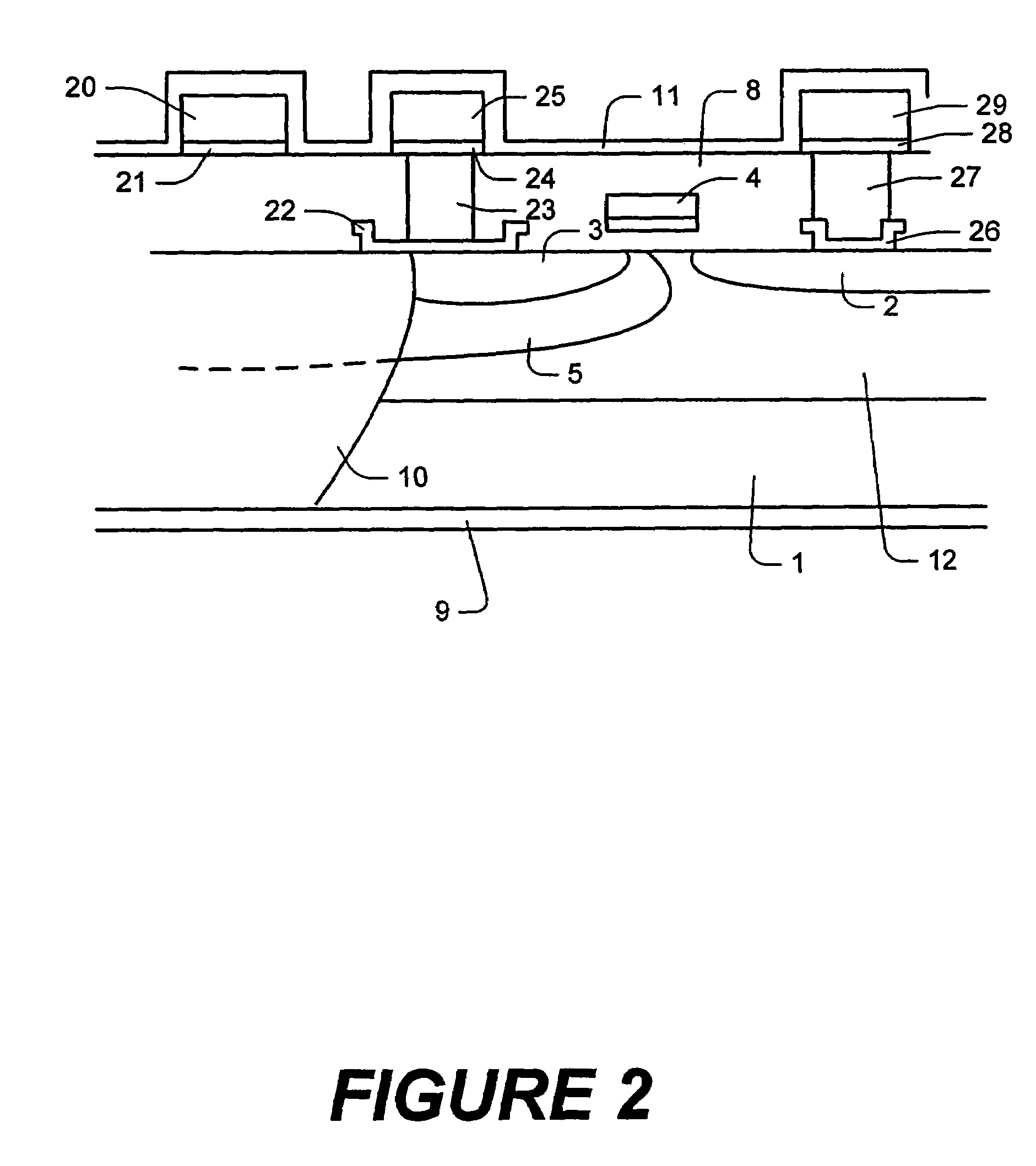
[0060]Turning to the drawings, exemplary embodiments of the present application will now be described. FIG. 2 depicts an exemplary n-p-n lateral field effect transistor, such as a lightly doped drain MOS transistor (LDMOS). Similar areas carry similar numerals with respect to a transistor according to the prior art as shown in FIG. 1. A different concept of forming and arranging the respective runners for drain, gate and source is used in this type of improved transistor structure. FIG. 2 shows again a p+ type substrate with a p− epitaxial layer 12 and a backside metal layer 9 consisting, for example, of gold. N-type Drain and source regions 2, 3 are provided within the p− epitaxial layer 12. The source region 3 is surrounded by a stronger doped p-well 5. Through ion implantation, a p+ sinker area 10 is created which reaches from the source contact down to the backside of the substrate. A drain runner 29 and a source runner 25 are deposited on the top of the oxide layer 8 above the ...


PUM


Abstract

A semiconductor device has a semiconductor substrate, an insulating layer on top of the substrate, a lateral field effect transistor with a drain region and a source region arranged in the substrate and a gate arranged above the substrate within the insulating layer, a drain runner arranged on top of the insulator layer above the drain region, a source runner arranged on top of the insulator layer above the source region, a gate runner arranged on top of the insulator layer outside an area defined by the drain runner and the source runner, a first coupling structure with a via for coupling the drain runner with the drain region, and a second coupling structure with a via for coupling the source runner with the source region.

Description

FIELD OF THE INVENTION[0001]The present application relates to an LDMOS transistor structure.BACKGROUND OF THE INVENTION[0002]LDMOS transistor structures are widely used as semiconductor devices for many types of transistor applications such as high voltage MOS field effect transistors. An LDMOS transistor comprises a lightly doped drain region to enhance the breakdown voltage. LDMOS transistors are, however, limited in their high frequency performance due to the feedback capacitance Cdg between the gate and the drain. FIG. 1 shows one type of an LDMOS transistor as known in the art. A wafer comprises for example a p+ substrate 1 with an epitaxial layer 12 which includes n-type areas 2 and 3 implanted on the surface to provide a drain and source region, respectively. The backside of the substrate 1 comprises a wafer backside metal layer 9 which can be made of gold or aluminum and is used for grounding and source contact purposes. The epitaxial layer 12 is usually covered with an ins...

Claims


Application Information

Patent Timeline
Patent Type & Authority Patents(United States)
IPC IPC(8): H01L31/119H01L21/336H01L23/48H01L23/485H01L29/417H01L29/423H01L29/45H01L29/76H01L29/78
CPCH01L23/481H01L29/41725H01L29/4175H01L29/41766H01L29/42372H01L29/66659H01L29/7835H01L29/456H01L2924/0002H01L2924/00
Inventor MA, GORDONAHRENS, CARSTEN
Owner INFINEON TECH AG
Why Eureka
Try Eureka