Synchronous signal transfer and processing device

a technology of synchronous signal and processing device, which is applied in the direction of generating/distributing signals, instruments, pulse techniques, etc., can solve the problems of inability to shorten the cycle time of clock signal clk, disadvantageous increase in and inability to reduce the number of components of logical gates. , to achieve the effect of sufficient time width and reliably transferring data

Inactive Publication Date: 2006-10-10
RENESAS ELECTRONICS CORP
View PDF9 Cites 13 Cited by
  • Summary
  • Abstract
  • Description
  • Claims
  • Application Information

AI Technical Summary

Benefits of technology

[0041]It is an object of the present invention to provide a synchronous data transfer and processing device cap

Problems solved by technology

However, if delay circuits DLa and DLb are arranged on the data transmission path, the number of components of logical gates disadvantageously increases and a layout area and power dissipation disadvantageously increases.
In this case, there is caused a probability that the data in the definite state cannot be latched and unascertained data is transferred to the latch circuit at the next stage, causing a malfunction.
Therefore, if delay time TD is increased, the cycle time of clock signal CLK cannot be shortened, making it impossible to achieve high-speed operat

Method used


Image

  • Synchronous signal transfer and processing device
  • Synchronous signal transfer and processing device
  • Synchronous signal transfer and processing device

Examples


first embodiment

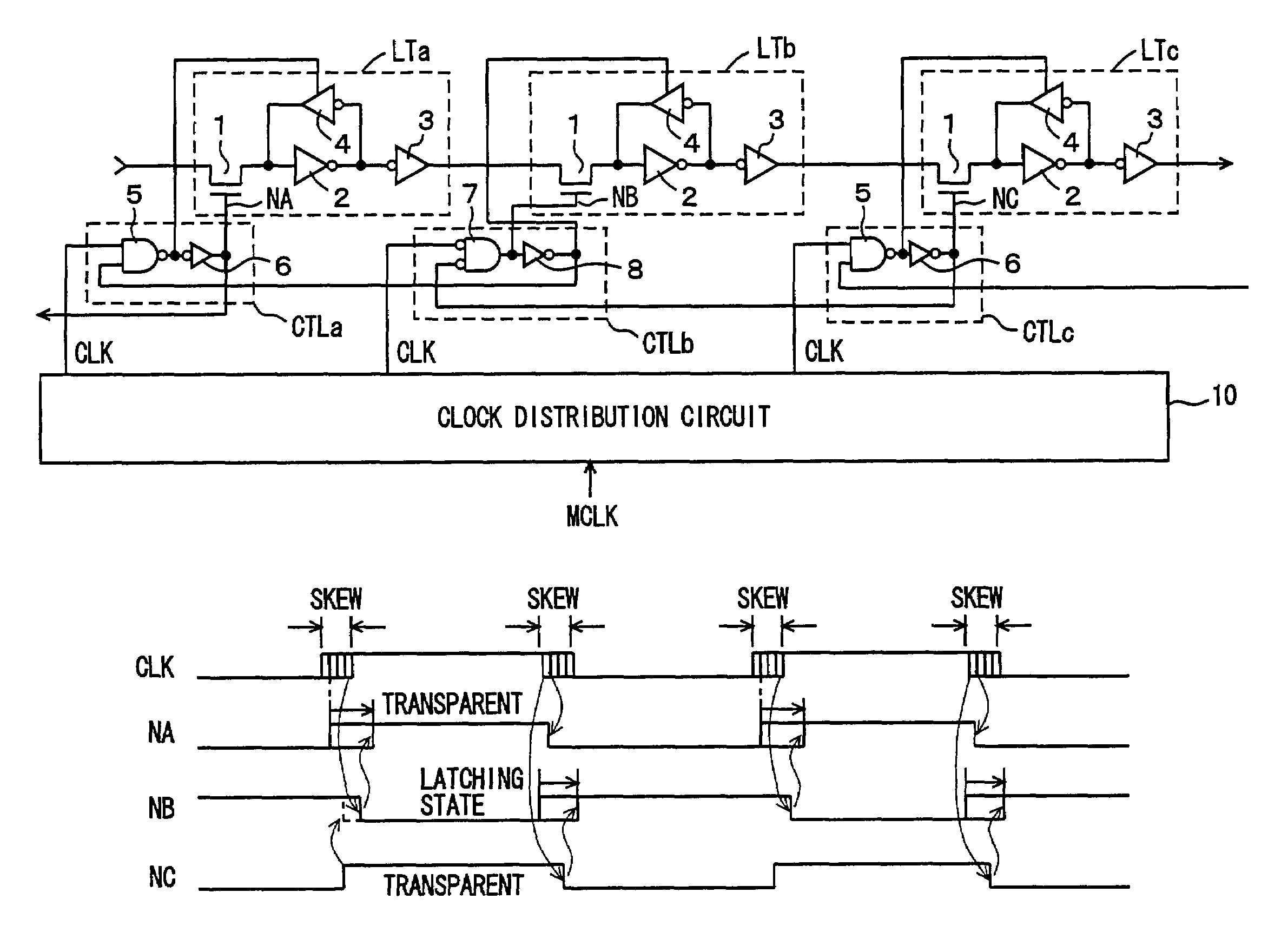
[0089]FIG. 1A is a schematic diagram showing a construction of a synchronous data transfer and processing device according to the first embodiment of the present invention. In FIG. 1A, latch circuits LTa to LTc cascaded in three stages are representatively shown. Clock control circuits CTLa to CTLc which generates control signals controlling the states (the latching state and the transparent state) of the corresponding latch circuits in accordance with clock signals CLK from a clock distribution circuit 10 and control signals for the latch circuits at the next stages, respectively are provided corresponding to latch circuits LTa to LTc, respectively.

[0090]Latch circuits LTa to LTc have the same configuration, and each includes a transfer gate 1 which selectively turns conductive in response to a control signal from corresponding clock control circuit CTLa, CTLb or CTLc, an inverter 2 which inverts data transmitted through transfer gate 1, an inverter 3 which inverts the output data ...

second embodiment

[0127]FIG. 4 is a block diagram of a synchronous data transfer and processing device according to the second embodiment of the present invention. In FIG. 4, this synchronous data transfer and processing device includes a plurality of cascaded multi-bit transfer circuits. In FIG. 4, multi-bit transfer circuits 15a to 15c cascaded in three stages are representatively shown. Multi-bit transfer circuit 15a includes latch circuits LTa0 to LTak which transmit input data DI0 to DIk, respectively in parallel. Multi-bit transfer circuit 15b includes latch circuits LTb0 to LTbk which are arranged corresponding to latch circuits LTa0 to LTak of multi-bit transfer circuit 15a, respectively. Multi-bit transfer circuit 15c include latch circuits LTc0 to LTck which are arranged corresponding to latch circuits LTb0 to LTbk of multi-bit transfer circuit 15b, respectively. These latch circuits LTa0 to LTb1, LTb0 to LTbk and LTc0 to LTck have the same configuration. Each of the latch circuits includes...

third embodiment

[0136]FIG. 5 is a schematic block diagram showing a configuration of a synchronous data transfer and processing device according to the third embodiment of the present invention. In FIG. 5, a logical circuit LGK is interposed between latch circuits LTi and Ltg. The signal propagation delay time of logical circuit LGK is longer than a clock skew.

[0137]If the number of logical stages of logical circuit LGK is great and the gate delay thereof is longer than a clock skew, a delay circuit for preventing racing is equivalently arranged in the signal / data transfer path and no racing problem occurs in latch circuits LTi and LTj. Therefore, a control signal is not fed back from clock control circuit CTLj provided for latch circuit LTj to clock control circuit CTLi provided for this latch circuit LTi. Clock control circuit CTLi controls the state of latch circuit LTi in accordance with corresponding clock signal CLK. On the other hand, since there is a possibility that a racing problem occurs...


PUM


Abstract

A transfer circuit includes a plurality of cascaded latch circuits. Two consecutive latch circuits in the transfer circuit complementarily enter a latching state and a transparent state in response to the applied clock signal, and data/a signal is transferred through the transfer circuit in response to the clock signal. A clock control circuit is provided for controlling an operation of each of the latch circuits. The clock control circuit detects that the latch circuit in a next stage of the corresponding latch circuit enters the latching state to permits transfer of the signal/data of the corresponding latch circuit to the subsequent stage in accordance with the corresponding clock signal. It is possible to prevent the data/signal from being transferred while the latch circuit at the next stage is in the transparent state to accurately transfer the data/signal. A clock synchronous data transfer and processing device reliably preventing racing is implemented with a simple circuit configuration.

Description

BACKGROUND OF THE INVENTION[0001]1. Field of the Invention[0002]The present invention relates to a synchronous signal transfer and processing device for transferring a signal / data in accordance with a clock signal. More specifically, the present invention relates to a configuration for avoiding racing on the signal transfer path of the synchronous type signal transfer and processing device.[0003]2. Description of the Background Art[0004]A clock synchronous processing scheme of transferring and processing a signal synchronously with a clock signal is normally employed for high speed signal / data processing. According to this synchronous processing scheme, data / signal is transferred and processed by controlling the operation state of a latch circuit or a flip-flop circuit for holding the data / signal in synchronization with a clock signal.[0005]The synchronous processing scheme for transferring and processing a signal synchronously with a clock signal allows a signal / data to be processe...

Claims


Application Information

Patent Timeline
IPC IPC(8): H04L7/00H04L27/00G06F1/10G11C7/00G11C19/00G11C19/28H03K5/00H03K5/135H03K5/15H03L7/00
CPCG06F1/10G11C19/00G11C19/28H03K5/135H03K5/1506H03L7/00H03K2005/00241
Inventor TAKATA, HIDEHIRO
Owner RENESAS ELECTRONICS CORP
Why Eureka
Try Eureka