Thin-film transistor with set trap level densities, and method of manufactures

a technology of thin film transistors and trap levels, which is applied in the direction of instruments, semiconductor devices, optics, etc., can solve the problems of deterioration in display performance, increased light leakage current problems, and large influence of generated light leakage current, so as to reduce light leakage, reduce leakage current, and reduce throughput without reducing the effect of throughpu

Inactive Publication Date: 2006-10-17
VISTA PEAK VENTURES LLC
View PDF14 Cites 7 Cited by
  • Summary
  • Abstract
  • Description
  • Claims
  • Application Information

AI Technical Summary

Benefits of technology

[0015]In a case where an insulating film of a high interfacial level is placed between the electroconductive film and the active layer to reduce the electrical influence of the electroconductive film on the active layer according to a conventional art, a leak current due to the electrical influence of the electroconductive film is reduced but the facility with which a channel is formed on the electroconductive film side of the channel region is simultaneously reduced, resulting in a reduction in drain current when the thin-film transistor is on. In the thin-film transistor of the present invention, the trap level density in the channel region in the surface portion of the active layer on the electroconductive film side is set equal to the trap level density in the surface of the active layer on the gate electrode side for example, and the trap level density in the source region and the drain region is set higher than the trap level density in the channel region in the surface portion of the active layer on the electroconductive film side, thereby reducing the leak current due to the electrical influence of the electroconductive film even in a case where the active layer and the electroconductive film are brought closer to each other, while avoiding a reduction in drain current when the thin-film transistor is on. The electroconductive film may be formed of a non-optically-transparent metal silicide, for example. Alternatively, the electroconductive film may be formed of silicon having a light absorbing property and doped with a carrier.
[0034]Since the TFT substrate of the present invention has the thin-film transistor of the present invention, it can be suitably used in a liquid crystal display device into which light enters at a comparatively high luminance from the counter substrate side. In the liquid crystal display device of the present invention, a high luminance and high contrast can be attained since the TFT substrate of the present invention is provided.

Problems solved by technology

When light enters this active layer, a light leak current is generated due to photoexciation to cause a reduction in contrast for example, resulting in deterioration in display performance.
In particular, in a case where an active-matrix liquid crystal display device is used as a light valve in a projection-type display apparatus, light enters the liquid crystal display device at a high luminance and the influence of a generated light leak current is large.
For this reason, the light leak current problem has become more serious.
However, if the light shielding film is brought close to the active layer, a problem arises that the light shielding film electrically influences the active layer so that a channel is formed in the active layer on the light shielding film side to cause another leak current on the back channel side of the TFT.
However, if this arrangement is adopted, the channel cannot be easily formed on the back channel side of the TFT even when a potential for turning on the TFT is applied to the gate electrode.
There is, therefore, a problem that the drain current when the TFT is on is also reduced, while the leak current is reduced.
As a result, the manufacturing process is complicated and the TFT manufacture throughput is reduced.

Method used


Image

  • Thin-film transistor with set trap level densities, and method of manufactures
  • Thin-film transistor with set trap level densities, and method of manufactures
  • Thin-film transistor with set trap level densities, and method of manufactures

Examples


first embodiment

(First Embodiment)

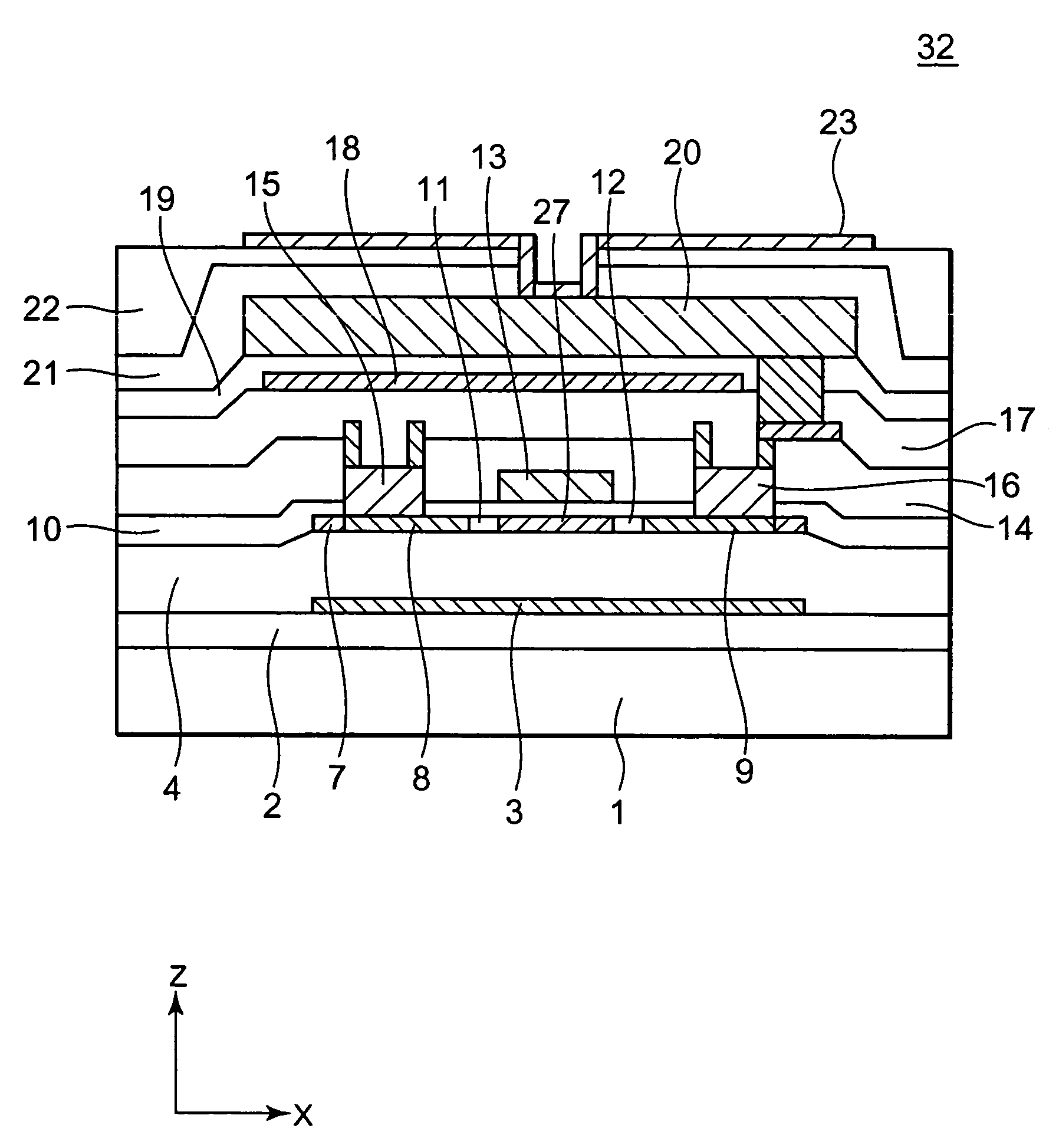
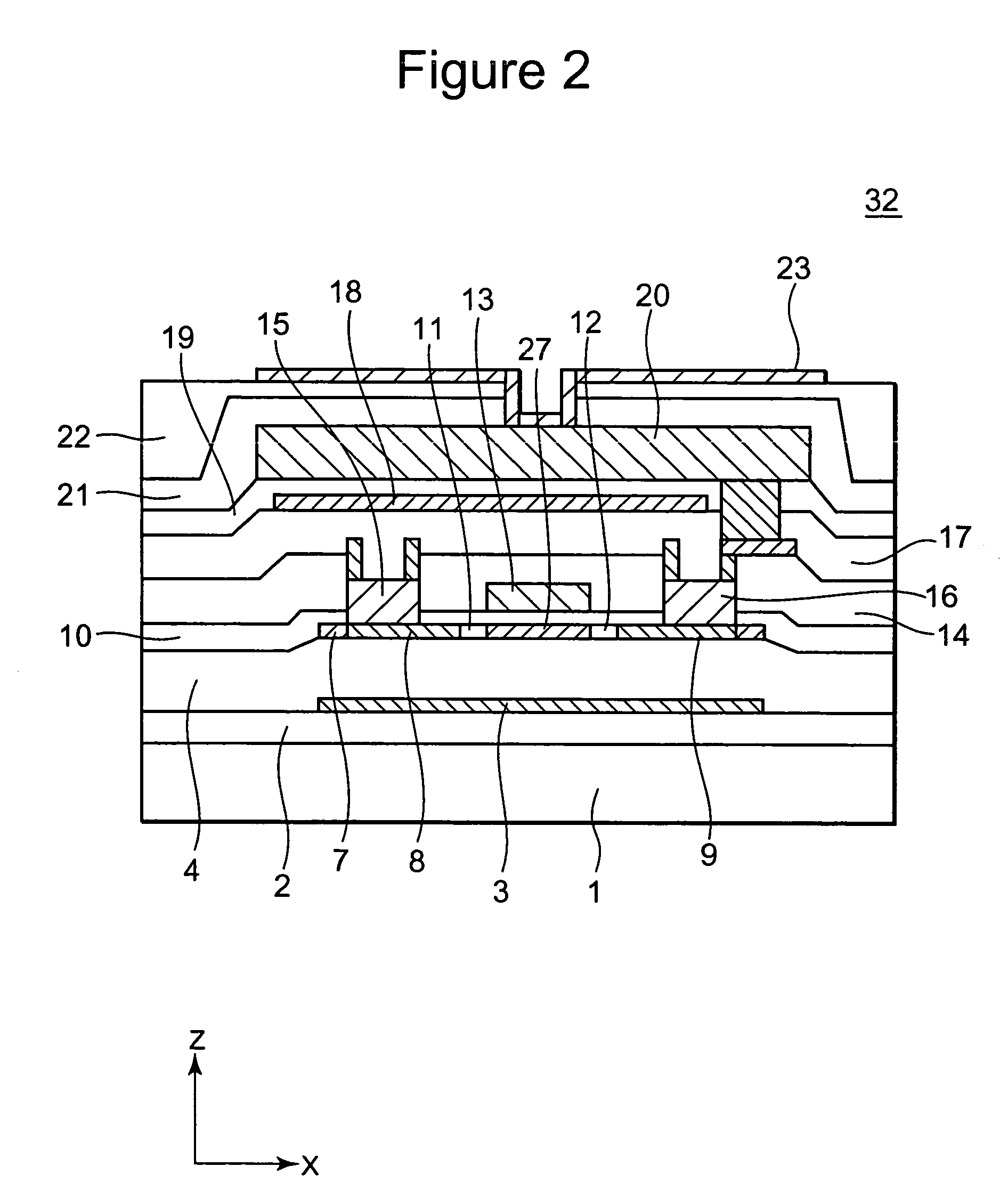
[0064]FIG. 1 shows a plan view of a portion of a thin-film transistor array substrate (TFT substrate) about a TFT in a liquid crystal display device in a first embodiment of the present invention, and FIG. 2 is a cross-sectional view taken along II—II of FIG. 1. The structure of the TFT substrate 32 constituting the active-matrix liquid crystal display device will be described in detail with reference to FIGS. 1 and 2. FIGS. 1 and 2 show one of a plurality of TFTs included in the TFT substrate 32. A black matrix 35 shown in FIG. 1 is omitted in FIG. 2.

[0065]As shown in FIG. 1, on the TFT substrate 32 are formed a plurality of data lines 28a extending along a Y-direction, a plurality of gate lines 26 extending along an X-direction, a plurality of TFTs 33 arranged in matrix form, and a black matrix 35 which shields the gate lines 26, the data lines 28a and the TFTs 33. The gate lines 26 are formed of a polysilicon film, a silicide film or the like doped with a carrie...

second embodiment

[0103]FIG. 10 shows one step in the process of manufacturing a TFT substrate in a second embodiment of the present invention. The process of manufacturing the TFT substrate 32 in this embodiment differs partly from that in the first embodiment. The TFT substrate in this embodiment has the same planar structure as that shown in FIG. 1 and the same sectional structure as that shown in FIG. 2. In the above-described first embodiment, electrical stress is applied after the formation of the TFT substrate 32 to introduce a trap level into the insulating film 4 and regions in the drain region 9 and the source region 8 at the interface between the insulating film 4 and the active layer 7. In this embodiment, a hydrogen plasma treatment is performed on the surface of the insulating film 4 before the formation of the active layer 7 on the insulating film 4 to damage the surface of the insulating film 4 on the active layer 7 side, thereby introducing a trap level into the interface between the...

third embodiment

[0109]FIG. 13 shows one step in the process of manufacturing a TFT substrate in a third embodiment of the present invention. The TFT substrate in this embodiment has the same planar structure as that shown in FIG. 1 and the same sectional structure as that shown in FIG. 2. In the above-described second embodiment, a hydrogen plasma treatment is performed on the surface of the insulating film 4 to introduce a trap level into the surface of the active layer 7 on the light shielding film 3 side. In the third embodiment, a carrier is implanted in the insulating film 4 to introduce a trap level into regions in the source region 8, the drain region 9 and the low-concentration carrier regions 11 and 12 in the surface of the active layer 7 on the light shielding film 3 side.

[0110]The TFT substrate 32 in this embodiment is fabricated as described below. The base insulating film 2 and the light shielding film 3 are formed on the glass substrate 1 in the same manner as shown in FIGS. 3(a) and ...


PUM

PropertyMeasurementUnit
current densityaaaaaaaaaa
thicknessaaaaaaaaaa
thicknessaaaaaaaaaa

Abstract

A light shielding film capable of shielding against light entering an active layer of a TFT and electroconductive is formed on the lower layer side of the active layer. Electrical stress is applied by causing a current in an insulating film between source and drain electrodes and the light shielding film to introduce a trap level at a density at least about 5×10¹² / cm2 into a source region and a drain region in a surface portion of the active layer on the light shielding film side.

Description

CROSS-REFERENCE TO RELATED APPLICATIONS[0001]The disclosure of Japanese Patent Application No. JP2003-273426 filed on Jul. 11, 2003 including the specification, drawings and abstract is incorporated herein by reference in its entirety.BACKGROUND OF THE INVENTION[0002]1. Field of the Invention[0003]The present invention relates to a thin-film transistor and a method of manufacturing the thin-film transistor. More particularly, the present invention relates to a thin-film transistor having an electroconductive film opposed to (i.e., facing) an active layer and a method of manufacturing the thin-film transistor. The present invention also relates to a TFT substrate and a liquid crystal display device. Further particularly, the present invention relates to a TFT substrate having a plurality of thin-film transistors of the present invention and to a liquid crystal display device having such a TFT substrate.[0004]2. Description of Related Art[0005]In recent years, the development of displ...

Claims


Application Information

Patent Timeline
Patent Type & Authority Patents(United States)
IPC IPC(8): G02F1/136G02F1/1362H01L21/336H01L27/12H01L29/786
CPCG02F1/136209H01L27/12H01L29/66757H01L29/78609H01L29/78618H01L29/78621H01L29/78633H01L29/78675H01L29/78696
Inventor MATSUNAGA, NAOKISERA, KENJI
Owner VISTA PEAK VENTURES LLC
Why Eureka
Try Eureka