Multi-layer band-pass filter

a band-pass filter and multi-layer technology, applied in the direction of coupling devices, electrical devices, waveguides, etc., can solve the problems of inability to adjust the characteristics of multi-layer dielectric filters, the loss of band-pass filters and baluns is greater, and the circuitry including the band-pass filter and the balun suffers greater loss, etc., to achieve the effect of easy adjustment of their characteristics

Active Publication Date: 2006-10-24
TDK CORPARATION
View PDF25 Cites 39 Cited by
  • Summary
  • Abstract
  • Description
  • Claims
  • Application Information

AI Technical Summary

Benefits of technology

[0019]It is an object of the invention to provide a multi-layer band-pass filter that is small-sized, capable of outputting balanced signals, and allows easy adjustment of its characteristics.
[0022]In the first multi-layer band-pass filter of the invention, the two balanced outputs are connected to the half-wave resonator for balanced output that is made up of a half-wave resonator having open-circuited ends. It is thereby possible to output balanced signals from the two balanced outputs without providing any balun. In this multi-layer band-pass filter, the capacitor made up of part of the multi-layer substrate is provided in at least one of a location between the unbalanced input and the input resonator and a location between each of the balanced outputs and the half-wave resonator for balanced output. According to this multi-layer band-pass filter, it is easy to adjust the capacitance of the capacitor, and therefore it is easy to adjust the filter characteristics.
[0027]As described above, the second multi-layer band-pass filter of the invention comprises the half-wave resonator for balanced output that is made up of a half-wave resonator having open-circuited ends, and one or more stages of the quarter-wave resonators for balanced output disposed between the half-wave resonator for balanced output and the balanced outputs. The two balanced outputs are connected to the pair of the quarter-wave resonators for balanced output of the final stage, respectively. As a result, according to the second multi-layer band-pass filter, it is possible to output balanced signals from the two balanced outputs without providing any balun. In this multi-layer band-pass filter, the capacitor made up of part of the multi-layer substrate is provided in at least one of a location between the unbalanced input and the resonator connected thereto and a location between each of the balanced outputs and the pair of the quarter-wave resonators of the final stage. According to this multi-layer band-pass filter, it is easy to adjust the capacitance of the capacitor, and therefore it is easy to adjust the filter characteristics.
[0034]As described above, according to the first multi-layer band-pass filter of the invention, the band-pass filter section incorporates, as the resonators, the input resonator to which the unbalanced input is connected, and the half-wave resonator for balanced output to which the balanced outputs are connected. The half-wave resonator for balanced output is made up of a half-wave resonator having open-circuited ends. The multi-layer band-pass filter of the invention comprises the multi-layer substrate used for integrating the resonators. In the multi-layer band-pass filter, the capacitor made up of part of the multi-layer substrate is provided in at least one of a location between the unbalanced input and the input resonator and a location between each of the balanced outputs and the half-wave resonator for balanced output. Because of these features of the invention, it is possible to implement the multi-layer band-pass filter that is capable of producing balanced signals, small-sized, and easy to adjust the characteristics.
[0035]According to the second multi-layer band-pass filter of the invention, the band-pass filter section incorporates, as the resonators, the half-wave resonator for balanced output that is made up of a half-wave resonator having open-circuited ends, and the quarter-wave resonators for balanced output each of which is made up of a quarter-wave resonator. The quarter-wave resonators for balanced output are provided to form one or more stages, each stage consisting of a pair of the quarter-wave resonators for balanced output. The quarter-wave resonators for balanced output are disposed between the half-wave resonator for balanced output and the balanced outputs. The balanced outputs are connected to the pair of the quarter-wave resonators of the final stage, respectively. The multi-layer band-pass filter of the invention comprises the multi-layer substrate used for integrating the resonators. In the multi-layer band-pass filter, the capacitor made up of part of the multi-layer substrate is provided in at-least one of a location between the unbalanced input and the resonator connected thereto and a location between each of the balanced outputs and the pair of the quarter-wave resonators of the final stage. Because of these features of the invention, it is possible to implement the multi-layer band-pass filter that is capable of producing balanced signals, small-sized, and easy to adjust the characteristics.

Problems solved by technology

Therefore, to give an output signal of this band-pass filter to a balanced-input amplifier, an unbalance-to-balance transformer (balun) is required for transforming an unbalanced signal to a balanced signal made up of two signals that are nearly 180 degrees out of phase with each other and have nearly equal amplitudes.
If the band-pass filter and the balun are made as discrete circuits, the number of components is large so that there arises a problem that the circuitry including the band-pass filter and the balun suffers greater loss and has greater dimensions.
Therefore, this multi-layer dielectric filter is not capable of solving the above-mentioned problem.
It is difficult to obtain a high capacitance in such a configuration because of the following reason.
However, it is difficult to increase the area of the terminal electrode in view of the size of the dielectric filter.
In addition, if the thickness of a portion of the dielectric block between the terminal electrode and the internal conductor is reduced, the ceramic of which the dielectric block is made is broken when fired.
It is therefore difficult to reduce the space between the terminal electrode and the internal conductor, too.
According to the dielectric filter disclosed in the Published Unexamined Japanese Patent Application 2000-349505, it is difficult to greatly change the area of the terminal electrode and the space between the terminal electrode and the internal conductor.
It is therefore difficult to adjust the capacitance produced between the terminal electrode and the internal conductor in this dielectric filter.
As described so far, it is difficult to adjust the filter characteristics, according to the dielectric filter disclosed in the Published Unexamined Japanese Patent Application 2000-349505.

Method used


Image

  • Multi-layer band-pass filter
  • Multi-layer band-pass filter
  • Multi-layer band-pass filter

Examples


first embodiment

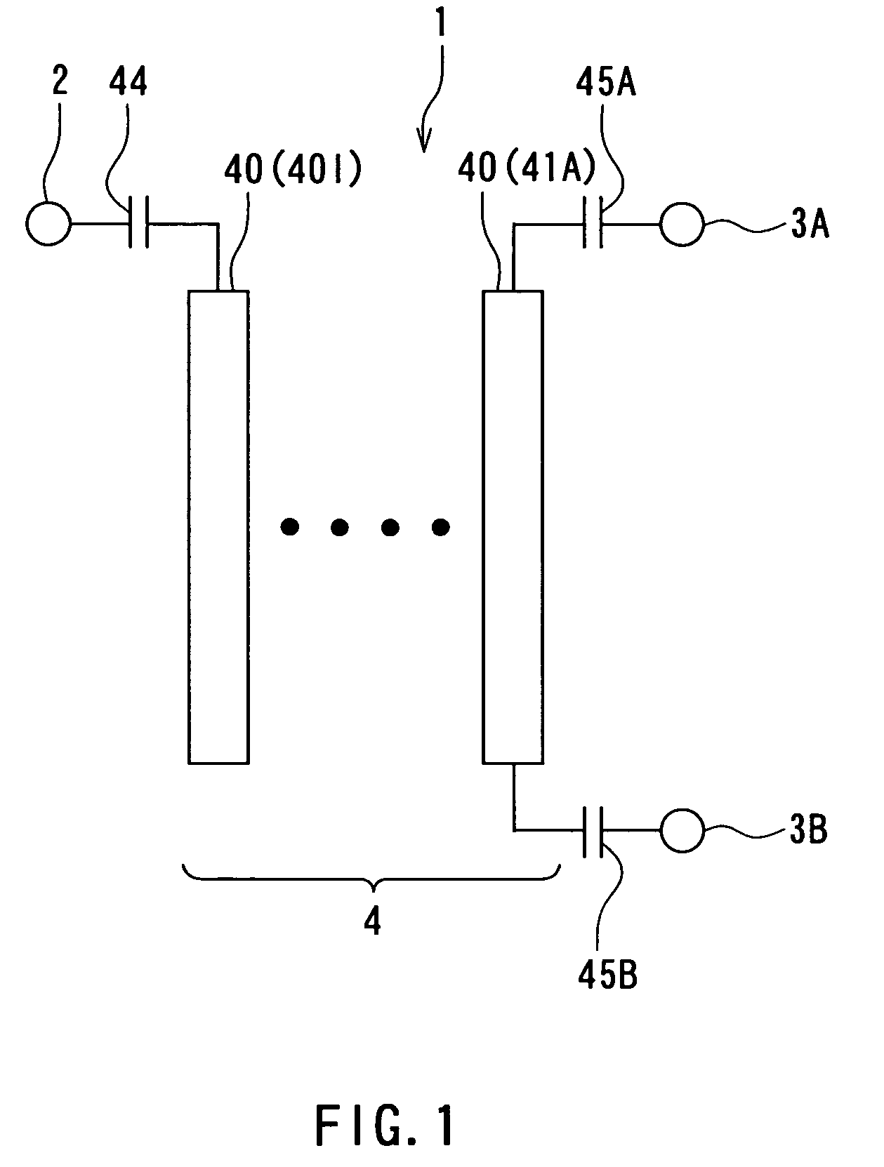
[0080]Reference is now made to FIG. 1 to describe a basic configuration of a multi-layer band-pass filter of a first embodiment of the invention. As shown in FIG. 1, the multi-layer band-pass filter 1 of the embodiment comprises: a single unbalanced input 2 for receiving unbalanced signals; two balanced outputs 3A and 3B for outputting balanced signals; and a band-pass filter section 4 provided between the unbalanced input 2 and the balanced outputs 3A and 3B. The band-pass filter section 4 incorporates a plurality of resonators 40 each of which is made up of a TEM line. The multi-layer band-pass filter 1 further comprises a multi-layer substrate used for integrating the resonators 40.

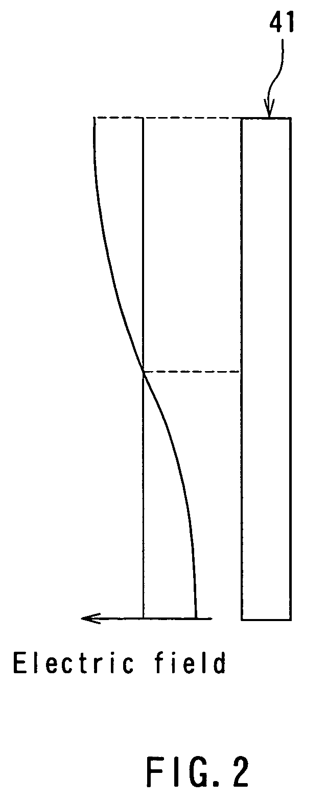
[0081]The band-pass filter section 4 incorporates, as the resonators 40, an input resonator 40I to which the unbalanced input 2 is connected, and a half-wave resonator 41A for balanced output to which the balanced outputs 3A and 3B are connected. The half-wave resonator 41A for balanced output is made ...

first configuration example

[0099]FIG. 8 is a schematic diagram of the multi-layer band-pass filter 1 of the first configuration example. The band-pass filter 1 comprises the unbalanced input 2, the balanced outputs 3A and 3B, and the band-pass filter section 4 provided between the unbalanced input 2 and the balanced outputs 3A and 3B. The band-pass filter section 4 incorporates three resonators 40 disposed side by side, each of which is made up of the resonator 41 having the open-circuited ends. Among the three resonators 40, the resonator 40 disposed closest to the unbalanced input 2 is the input resonator 40I. The unbalanced input 2 is connected to the input resonator 40I through the capacitor 44. The resonator 40 disposed closest to the balanced outputs 3A and 3B is the half-wave resonator 41A. The balanced outputs 3A and 3B are connected to the half-wave resonator 41A through the capacitors 45A and 45B, respectively. The resonator 40 disposed between the resonator 40I and the resonator 41A will be hereina...

second configuration example

[0107]FIG. 11 is a schematic diagram of the multi-layer band-pass filter 1 of the second configuration example. According to this band-pass filter 1, a direct current voltage application terminal 5 is added to the band-pass filter 1 of the first configuration example of FIG. 8. The direct current voltage application terminal 5 is directly connected to a portion of the half-wave resonator 41A for balanced output near the middle of the length of the half-wave resonator 41A. In the second example, the balanced output 3A is directly connected to one half portion of the half-wave resonator 41A taken along the length thereof The balanced output 3B is directly connected to the other half portion of the half-wave resonator 41A taken along the length thereof. The terminal 5 is used to apply a direct current voltage to the resonator 41A. This direct current voltage is used to drive integrated circuits connected to the balanced outputs 3A and 3B, for example.

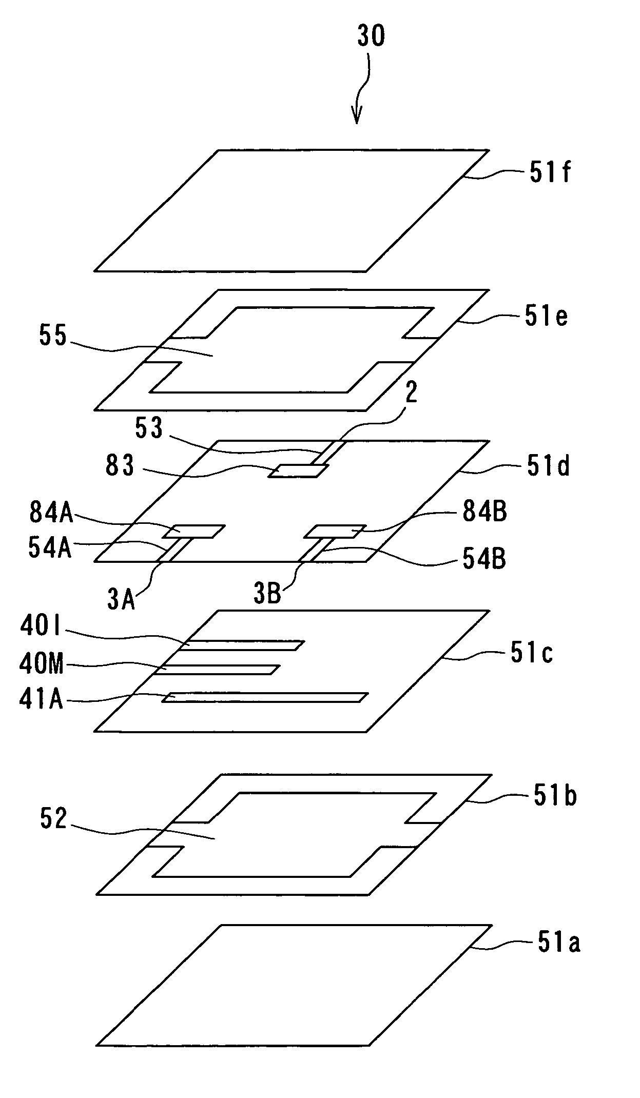
[0108]FIG. 12 is an exploded perspe...


PUM


Abstract

A multi-layer band-pass filter comprises an unbalanced input, two balanced outputs, and a band-pass filter section provided between the unbalanced input and the two balanced outputs. The band-pass filter section incorporates a plurality of resonators each of which is made up of a TEM line. The band-pass filter further comprises a multi-layer substrate used for integrating the resonators. The band-pass filter section incorporates, as the resonators, an input resonator, and a half-wave resonator for balanced output that is made up of a half-wave resonator having open-circuited ends. The unbalanced input is connected to the input resonator through a capacitor. Each of the balanced outputs is connected to the half-wave resonator through a capacitor.

Description

BACKGROUND OF THE INVENTION[0001]1. Field of the Invention[0002]The present invention relates to a multi-layer band-pass filter having balanced outputs.[0003]2. Description of the Related Art[0004]Reductions in size and thickness of radio communications devices such as cellular phones have been strongly sought, and techniques for mounting components with higher density have been therefore required. Integration of components through the use of a multi-layer substrate has been thus proposed.[0005]One of the components of radio communications devices is a band-pass filter for filtering reception signals. A known type of such a band-pass filter is a multi-layer band-pass filter as disclosed in the Published Unexamined Japanese Patent Application 2003-87008. This multi-layer band-pass filter comprises a resonator made up of conductor layers of a multi-layer substrate.[0006]A conventional multi-layer band-pass filter is designed to receive and output unbalanced signals of which ground pot...

Claims


Application Information

Patent Timeline
Patent Type & Authority Patents(United States)
IPC IPC(8): H01P1/20H01P1/203H01P5/10
CPCH01P1/20345H01P5/10H01P1/20
Inventor FUKUNAGA, TATSUYAMATSUBARA, HIDEYATODA, SHINICHIROH
Owner TDK CORPARATION
Why Eureka
Try Eureka