Electro-optical device

a technology of optical devices and optical buffer layers, applied in the field of optical buffer layers, can solve the problems of reducing system efficiency, long-term (bias) drift, and inability to avoid the buffer layer underneath the bias electrode, so as to reduce the overall length of the device, eliminate the effect of long-term drift effect and improve design efficiency

Active Publication Date: 2006-10-24
OCLARO NORTH AMERICA
View PDF5 Cites 21 Cited by
  • Summary
  • Abstract
  • Description
  • Claims
  • Application Information

AI Technical Summary

Benefits of technology

[0011]One advantage of the disclosed electro-optical device is that the design effectively eliminates the long-term drift effect found in prior art devices. Another advantage is that certain elements of the disclosed device are positioned relative to one another such that spacing between the elements as well as the overall length of the device are reduced, resulting in a more efficient design that, among other things, requires less operating power relative to prior art devices.

Problems solved by technology

Unfortunately, with this design it is not possible to avoid the having the buffer layer underneath the bias electrode, which is disadvantageous in terms of long-term (bias) drift.
Further, positioning the bias electrode on top of the buffer layer increases the distance between the electrodes and the optical waveguides, reducing the efficiency of the system and making it unsuitable for high-efficiency applications.

Method used


Image

  • Electro-optical device
  • Electro-optical device
  • Electro-optical device

Examples


Embodiment Construction

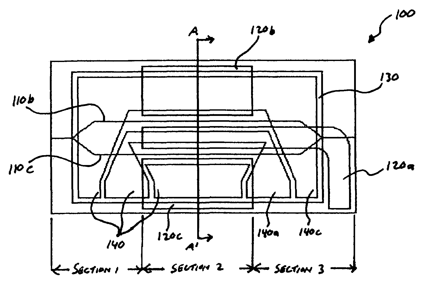
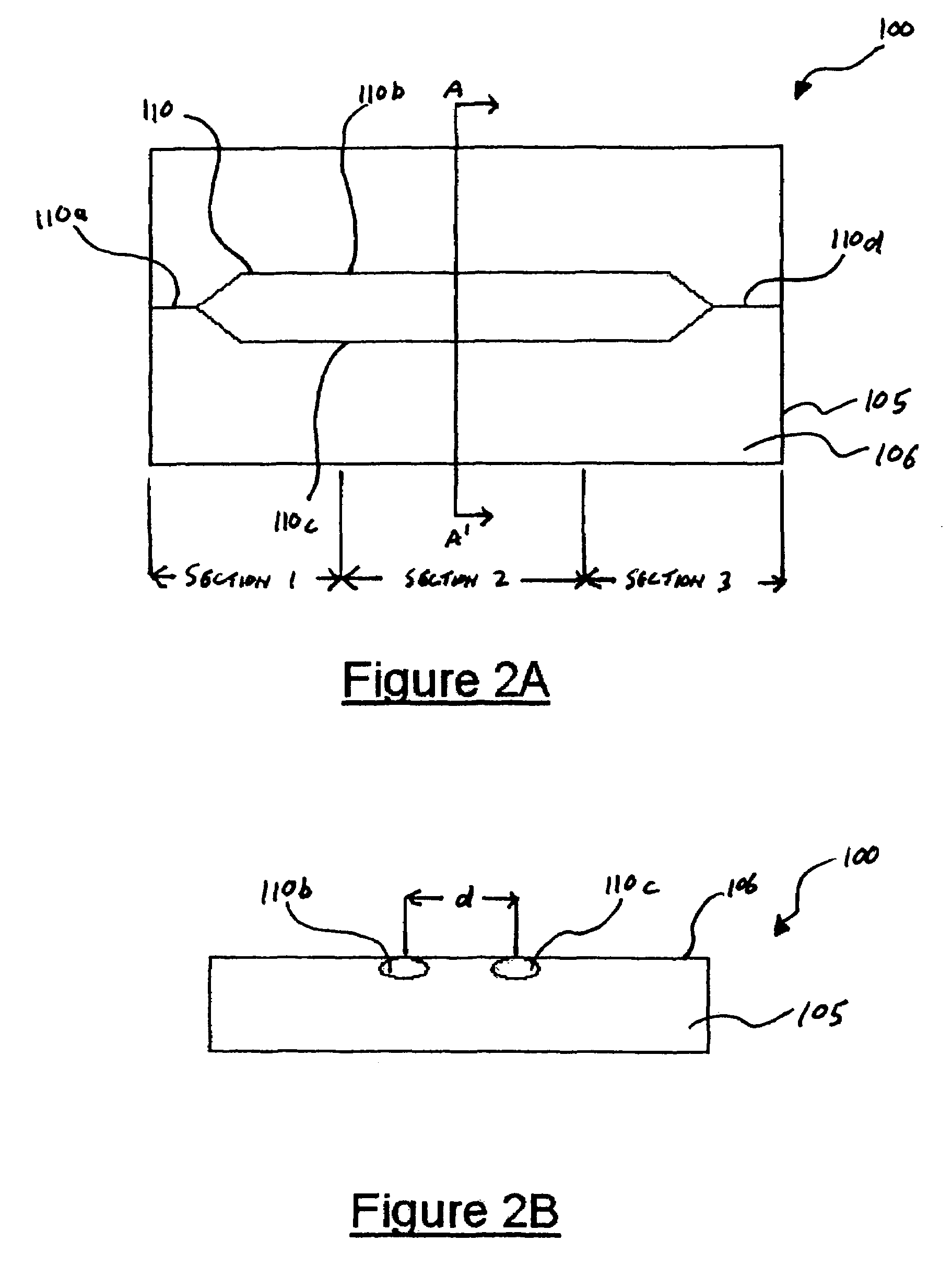
[0022]Referring now to FIG. 2A, there is shown an electro-optical device 1 having a substrate 5 with an embedded optical waveguide 10 relative to the corresponding top surface 6. The optical waveguide 10 is divided into 3-sections. In Section 1, the optical waveguide 10 includes a linear portion having a single optical pathway 10a, which forks into two parallel optical pathways 10b, 10c. Section 2 includes the two parallel optical pathways 10b, 10c traversing laterally across the substrate 5 relative to the top surface 6. In Section 3, the parallel optical pathways 10b, 10c converge to reform a single optical pathway 10d. The substrate 5 is formed of a suitable material such as Libnium Niobate (LiNbO3). The optical waveguide 10 is formed of a suitable material having an optical field that is sensitive to, or can be manipulated by, and electromagnetic field. Though FIG. 2A shows an x-cut LiNbO3, the present invention may be applied to other material cuts as well.

[0023]FIG. 2B shows a...


PUM

PropertyMeasurementUnit
thicknessaaaaaaaaaa
thicknessaaaaaaaaaa
thicknessaaaaaaaaaa

Abstract

Accordingly, a preferred embodiment of the present invention comprises an electro-optical device having an optical waveguide that includes two optical pathways, wherein the optical waveguide is embedded within the substrate. A bias electrode layer is formed on the surface of the substrate. A buffer layer is formed on at least a portion of the bias electrode layer and the surface of the substrate. An RF electrode layer is formed on the buffer layer. A bias-tee electrically couples the bias electrode layer and the RF electrode layer.

Description

BACKGROUND OF THE INVENTION[0001]1. Field of the Invention[0002]The present invention relates generally to electro-optical devices, and more specifically to electro-optical devices suitable for phase / intensity modulation and switching.[0003]2. Description of the Related Art[0004]Phase / intensity modulators and switches using an electro-optic material are in common use in the Telecom industry. An optical-electrical device, such as a Mach-Zehnder interferometer, can be used to bias an optical signal. These devices are typically driven by both a bias voltage, which sets the operating point, and an RF voltage, which is responsible for the actual modulation.[0005]FIG. 1A shows a first prior-art Mach-Zehnder type electro-optical device 1. An optical waveguide 10 is embedded in the top surface 6 of a substrate 5. The substrate 5 is an x-cut LiNbO3 material. The optical waveguide 10 forks into two parallel optical pathways which later rejoin into a single optical pathway. The active regions ...

Claims


Application Information

Patent Timeline
Patent Type & Authority Patents(United States)
IPC IPC(8): G02F1/035G02B6/10
CPCG02F1/0316G02F1/035
Inventor BELMONTE, MICHELEPRUNERI, VALERIO
Owner OCLARO NORTH AMERICA
Why Eureka
Try Eureka