Large substrate test system

a technology for testing systems and substrates, applied in semiconductor/solid-state device testing/measurement, fault location by increasing destruction at fault, etc., can solve the problems of increasing shipping costs, high equipment ownership costs, and large equipment footprints

Inactive Publication Date: 2006-10-31
APPLIED MATERIALS INC
View PDF40 Cites 16 Cited by
  • Summary
  • Abstract
  • Description
  • Claims
  • Application Information

AI Technical Summary

Problems solved by technology

However, as testing equipment is increased in size to accommodate larger flat panels, simple scaling of current equipment designs would result in disadvantageously large equipment footprints.
Correspondingly, larger equipment footprint per processing

Method used


Image

  • Large substrate test system
  • Large substrate test system
  • Large substrate test system

Examples


Embodiment Construction

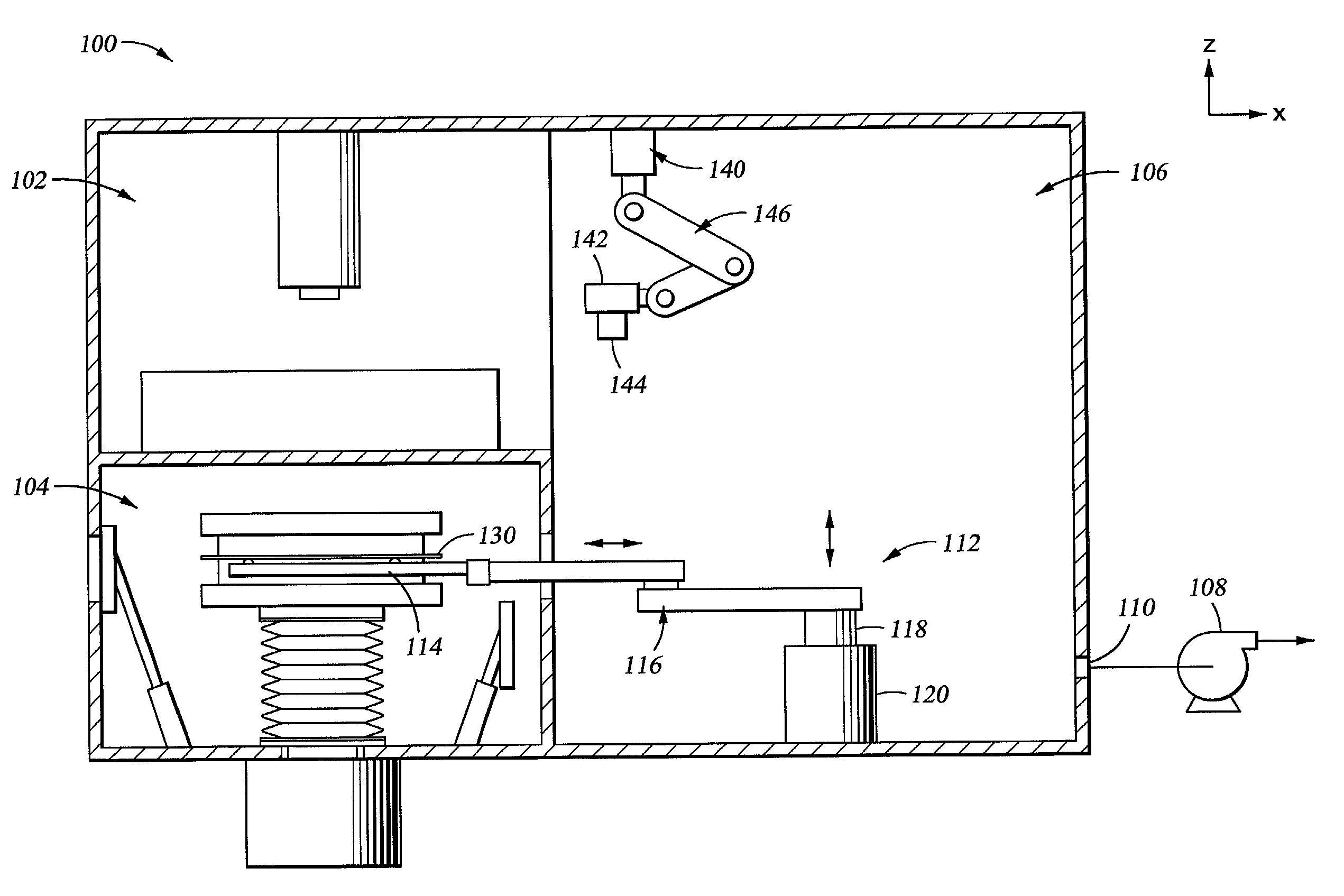
[0031]Embodiments of the present invention generally provide a method and system for testing and / or inspecting large substrates, such as those used to make flat panel thin film transistor displays. Although the test systems described herein provide a compact footprint as compared to known conventional systems for large area substrates, aspects of the space-saving and other features of the test systems may be readily incorporated into other test systems configured to process substrates of other types and sizes.

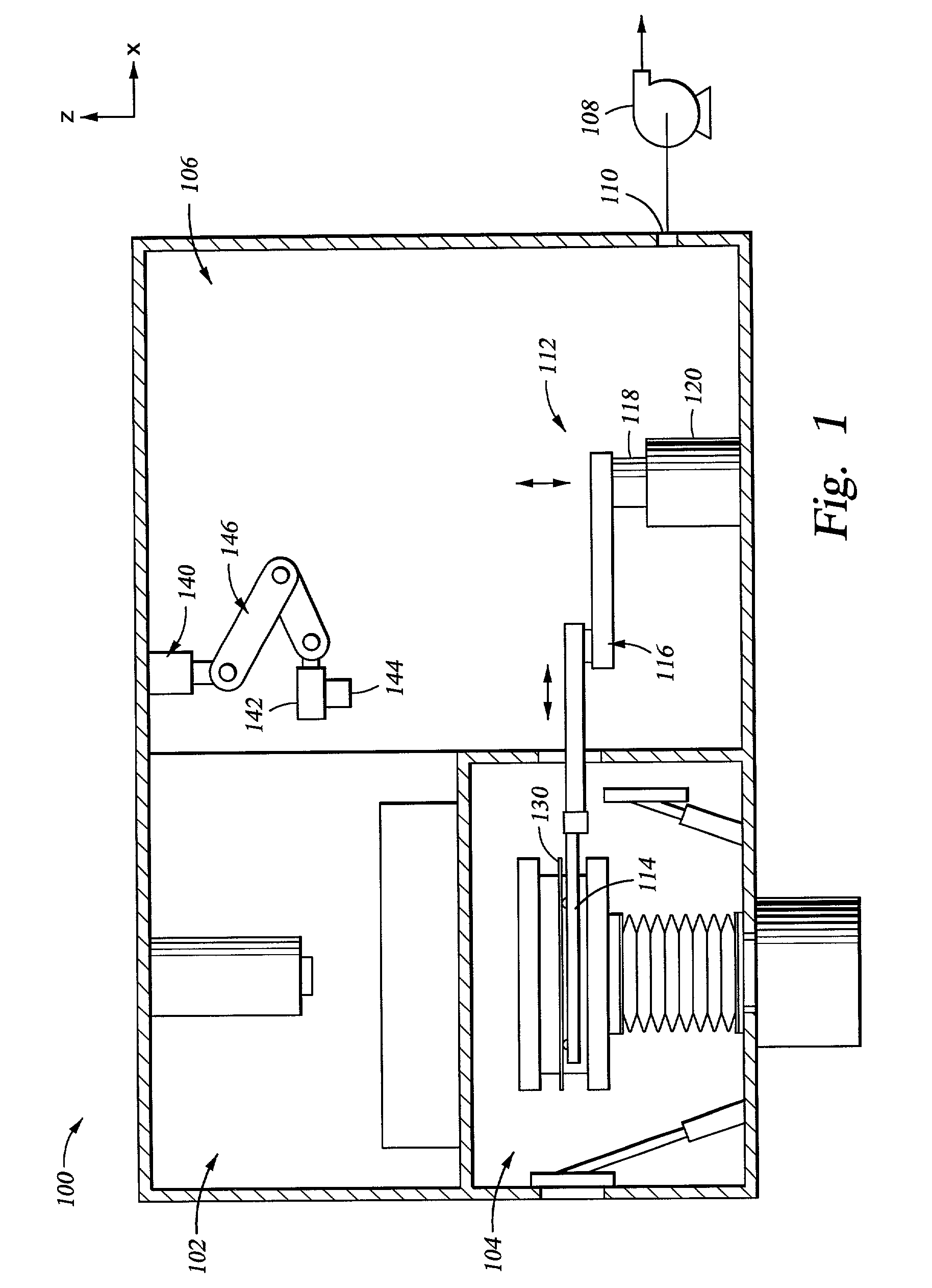
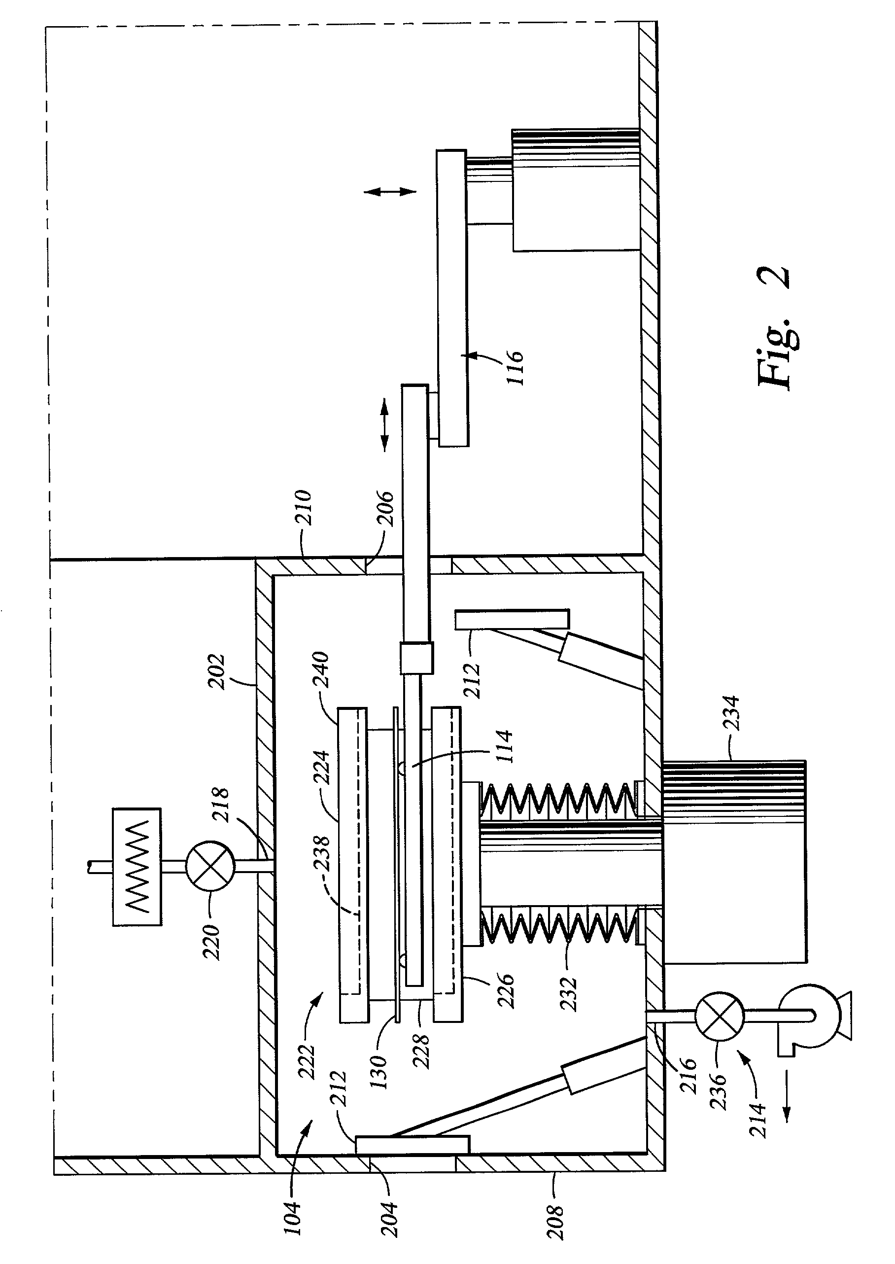
[0032]FIG. 1 depicts one embodiment of a test system 100 for testing and / or inspecting large area glass substrates. The test system 100 generally includes a test station 102, a load lock chamber 104 and a transfer chamber 106 for transferring substrates between the load lock chamber 104 and the test station 102. At least a portion of the test station 102 is mounted above the load lock chamber 104. The transfer chamber 106 is disposed adjacent the load lock chamber 104 and the t...


PUM


Abstract

A system and method for testing substrates is generally provided. In one embodiment, a test system for testing a substrate includes a load lock chamber, a transfer chamber and a test station. The load lock chamber and the test station are disposed on top of one another and coupled to the transfer chamber. The transfer chamber includes a robot adapted to transfer a substrate between the load lock chamber, which is at a first elevation, and the test station, which is at a second elevation. In another embodiment, a test station is provided having a turntable adapted to rotate the substrate. The turntable enables the range of motion required to test the substrate to be substantially reduced while facilitating full test and/or inspection of the substrate.

Description

BACKGROUND OF THE INVENTION[0001]1. Field of the Invention[0002]Embodiments of the invention generally relate to processing systems for large substrates.[0003]2. Background of the Related Art[0004]Thin film transistors (TFT) are commonly used for active matrix displays such as computer and television monitors, cell phone displays, personal digital assistants (PDAs), and an increasing number of other devices. Generally, flat panels comprise two glass plates having a layer of liquid crystal materials sandwiched therebetween. At least one of the glass plates includes one conductive film disposed thereon that is coupled to a power source. Power, supplied to the conductive film from the power source, changes the orientation of the crystal material, creating a pattern display.[0005]With the marketplace's acceptance of flat panel technology, the demand for larger displays, increased production and lower manufacturing costs have driven equipment manufacturers to develop new systems that acc...

Claims


Application Information

Patent Timeline
IPC IPC(8): G01R31/28G02F1/13G01R31/01H01L21/00H01L21/02H01L21/677H01L21/68
CPCH01L21/682H01L21/67748H01L21/67288G01R31/01H01L22/00
Inventor BRUNNER, MATTHIASKURITA, SHINICHIBLONIGAN, WENDELL T.KEHRBERG, EDGAR
Owner APPLIED MATERIALS INC
Why Eureka
Try Eureka