Method of reducing fringing capacitance in a MOSFET

a technology of mosfet and fringing capacitance, which is applied in the direction of basic electric elements, semiconductor devices, electrical apparatus, etc., to achieve the effect of reducing the fringing capacitance of mosfet devices and reducing oxide thickness

Active Publication Date: 2006-11-07
NAT SEMICON CORP
View PDF2 Cites 19 Cited by
  • Summary
  • Abstract
  • Description
  • Claims
  • Application Information

AI Technical Summary

Benefits of technology

[0003]According to the invention there is provided a method of reducing the fringing capacitance of a MOSFET device, comprising forming an air spacer on one or both sides of the gate of the device. This may include first forming an oxide liner and optionally a nitride spacer along both sides of the gate, as is known in the art, depositing an additional oxide layer, for at least one side of the gate, etching away at least part of one or both of the nitride spacer and oxide liner to leave a trench on the at least one side of the gate, and plugging the top of the trench to define an air spacer. The method may include etching back the additional oxide layer to expose upper ends of the nitride spacers. The method may further include forming a silicide layer on the gate and on the outside of the spacers formed by the oxide liner and nitride spacer prior to depositing the additional oxide layer and using the silicide layer as an etch-stop layer during etching back of the additional oxide layer. The etching away of at least part of one or both of the nitride spacer and oxide liner may include a selective nitride wet etch and a selective oxide wet etch. Preferably the nitride spacer is etched away entirely and the oxide liner is dipped off to reduce oxide thickness at the bottom corner adjacent the gate. The plugging of the trench may include depositing a thin oxide layer over the trench.

Problems solved by technology

However, since this also increases source and drain resistance, the oxide liner has typically been limited to a thickness of about 200 Å and the nitride spacer thickness or length to about 1000 Å.

Method used


Image

  • Method of reducing fringing capacitance in a MOSFET
  • Method of reducing fringing capacitance in a MOSFET

Examples


Embodiment Construction

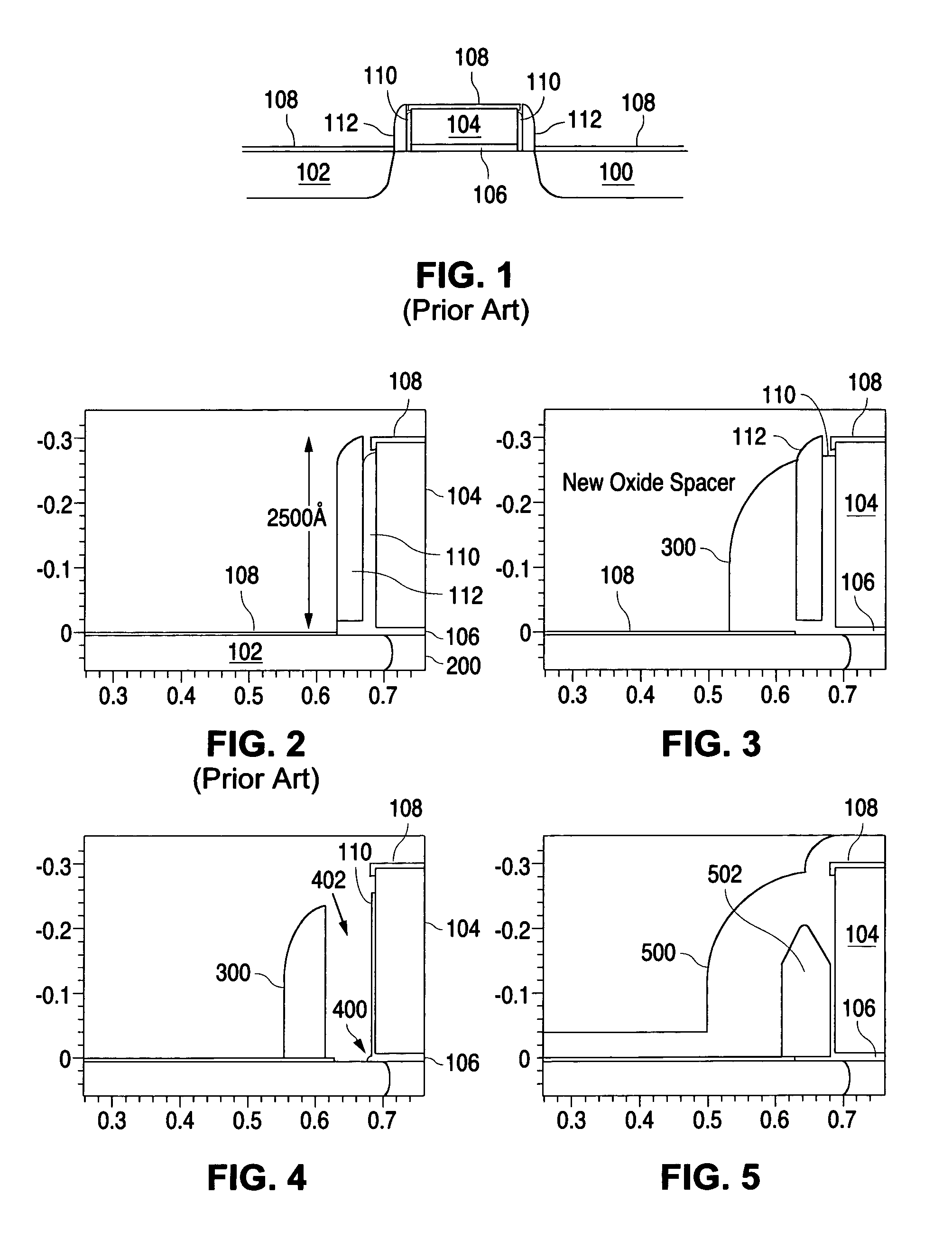
[0007]FIG. 2 shows an enlarged view of the left hand side of a typical MOSFET as known in the art just after silicidation in which a silicide layer 108 is formed on all silicon regions, including the polysilicon gate 104 and the source 102 (the drain 100 is not shown in FIG. 2). A typical MOSFET at this stage of the process includes a gate oxide layer 106 between the polysilicon gate 104 and the substrate 200.

[0008]As discussed above, typical MOSFET at this stage of the process includes a gate oxide layer 106 between the gate poly of gate 104 and the substrate 200. It also includes a spacer on both sides of the gate 104 (only the left hand spacer is shown in FIG. 2). Each spacer includes an oxide liner 110 and a nitride spacer 112.

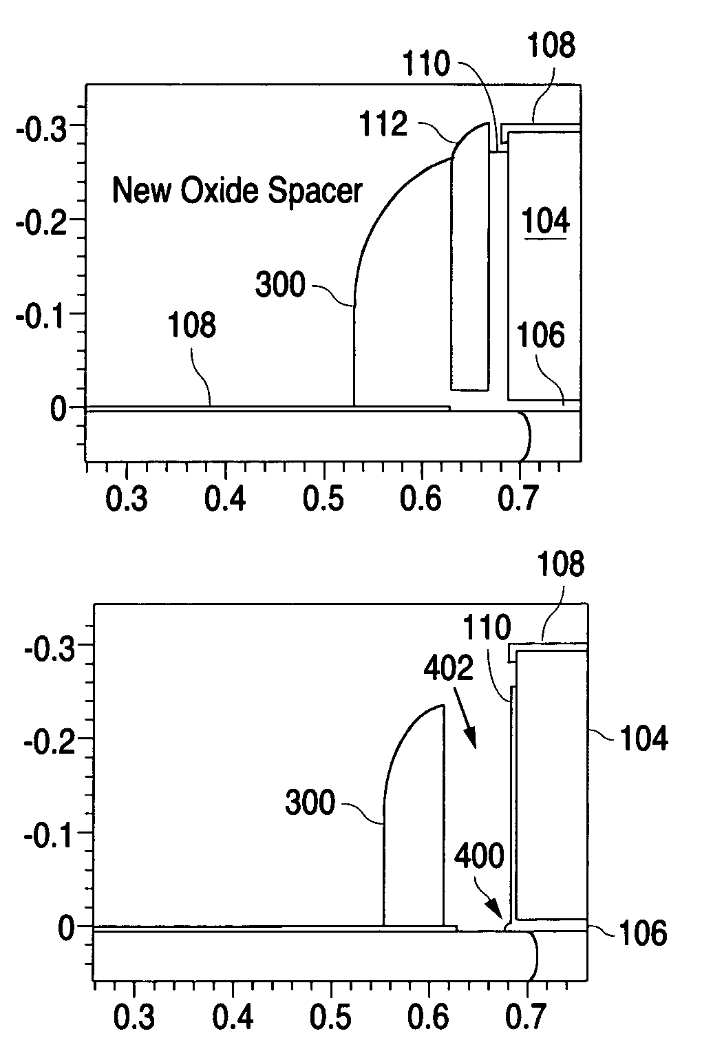
[0009]According to the invention, an extra oxide layer is deposited at this stage and is then etched back using the silicide layer 108 as an etch stop, thereby defining a new oxide spacer 300 as shown in FIG. 3.

[0010]The nitride spacer 112 is then etched a...


PUM


Abstract

In a method of reducing the fringing capacitance of a MOSFET, the nitride spacers on the sides of the MOSFET gate are etched away to form trenches, which are plugged to define air spacers.

Description

FIELD OF THE INVENTION[0001]The invention relates to MOSFET devices. In particular it relates to a method of reducing gate-source and gate-drain capacitance in a MOSFET device.BACKGROUND OF THE INVENTION[0002]As shown in FIG. 1, standard CMOS devices typically include a drain region 100 and a source region 102 formed on either side of a polysilicon gate 104, which is separated from the substrate by an oxide layer 106. Contact to the drain 100 and source 102 is achieved through a silicide layer 108. To ensure that the gate 104 and drain and source silicide 108 are not shorted a spacer is formed on either side of the gate 104 prior to forming the drain region 100 and source region 102 and prior to silicidation. Each spacer comprises an oxide liner 110 and a nitride spacer 112 as shown in FIG. 1. Since the bottom portions of the spacers adjacent the polysilicon gate 104 largely dictate the gate-drain capacitance and gate-source capacitance (also referred to as the fringing capacitance)...

Claims


Application Information

Patent Timeline
Patent Type & Authority Patents(United States)
IPC IPC(8): H01L21/336
CPCH01L29/4983H01L29/6653H01L29/78H01L29/4991
Inventor SADOVNIKOV, ALEXEIJOHNSON, PETER
Owner NAT SEMICON CORP
Why Eureka
Try Eureka