
Semiconductor device and method for manufacturing the same

Inactive Publication Date: 2005-08-11
FUJITSU LTD
View PDF23 Cites 2 Cited by
  • Summary
  • Abstract
  • Description
  • Claims
  • Application Information

AI Technical Summary

Benefits of technology

[0005] An object of the present invention is to provide such a semiconductor device as to reduce fringe capacitance in the most effective manner and to deter an escape of the above-mentioned impurity as much as possible, as well as to have a relatively simple manufacturing, and to provide a method for manufacturing the same.

Problems solved by technology

This causes to increase fringe capacitance, that is, parasitic capacitance generated mainly between a gate electrode and a semiconductor substrate, which is seen as a problem.
The above-described conventional art is effective to a great extent in reducing the fringe capacitance, but then in the first place, forming the cavity is not a simple task, and further an impurity introduced into the gate electrode in order to facilitate threshold voltage control tends to escape from the cavity in heat treatment processes thereafter.

Method used


Image

  • Semiconductor device and method for manufacturing the same
  • Semiconductor device and method for manufacturing the same
  • Semiconductor device and method for manufacturing the same

Examples


first embodiment

[0029] This embodiment discloses a structure of a semiconductor device that has a MOS transistor structure having a gate electrode, a source, and a drain, and a method for manufacturing the same. Here, the MOS transistor structure is explained together with its manufacturing process for convenience.

[0030]FIGS. 5A to 5G are schematic sectional views showing, in a process order, a method for manufacturing the MOS transistor relating to this embodiment.

[0031] First, as shown in FIG. 5A, a polycrystalline silicon film (not shown) is deposited on, for example, a p-type silicon semiconductor substrate 11 via a gate insulation film 12 by a CVD method or the like, and patterning of the polycrystalline silicon film and the gate insulation film 12 into an electrode shape causes to form a gate electrode 13.

[0032] Next, as shown in FIG. 5B, for example, a silicon oxide film (not shown) is deposited on the semiconductor device 11 by the CVD method or the like to cover the gate electrode 13, a...

second embodiment

[0039]FIGS. 6A to 6F are schematic sectional views showing, in a process order, a method for manufacturing a MOS transistor relating to this embodiment.

[0040] First, as shown in FIG. 6A, a polycrystalline silicon film (not shown) is deposited on, for example, a p-type silicon semiconductor substrate 11 via a gate insulation film 12 by a CVD method or the like, and patterning of the polycrystalline silicon film and the gate insulation film 12 into an electrode shape causes to form a gate electrode 13.

[0041] Next, as shown in FIG. 6B, for example, a silicon oxide film (not shown) is deposited on the semiconductor device 11 by the CVD method or the like to cover the gate electrode 13, and full anisotropic etching (etch back) of this silicon oxide film causes to form thin first films 14a only on side surfaces of the gate electrode 13 and the gate insulation film 12.

[0042] Next, as shown in FIG. 6C, only lower portions of the first films 14a are selectively removed by, for example, we...

third embodiment

[0047]FIGS. 7A to 7F are schematic sectional views showing, in a process order, a method for manufacturing a MOS transistor relating to this embodiment.

[0048] First, as shown in FIG. 7A, a polycrystalline silicon film (not shown) is deposited on, for example, a p-type silicon semiconductor substrate 11 via a gate insulation film 12 by a CVD method or the like, and patterning of the polycrystalline silicon film and the gate insulation film 12 into an electrode shape causes to form a gate electrode 13.

[0049] Next, as shown in FIG. 7B, side wall lower portions of the gate electrode 13 and a part of the gate insulation film 12 are removed by etching to make it notch-shaped. The notch sections become low permittivity regions 18.

[0050] Next, as shown in FIG. 7C, ion implantation of an n-type impurity such as phosphorus (P) is performed using the gate electrode 13 as a mask, to form a pair of extension regions 16 on a surface layer of the semiconductor substrate 11.

[0051] Next, as show...


PUM


Abstract

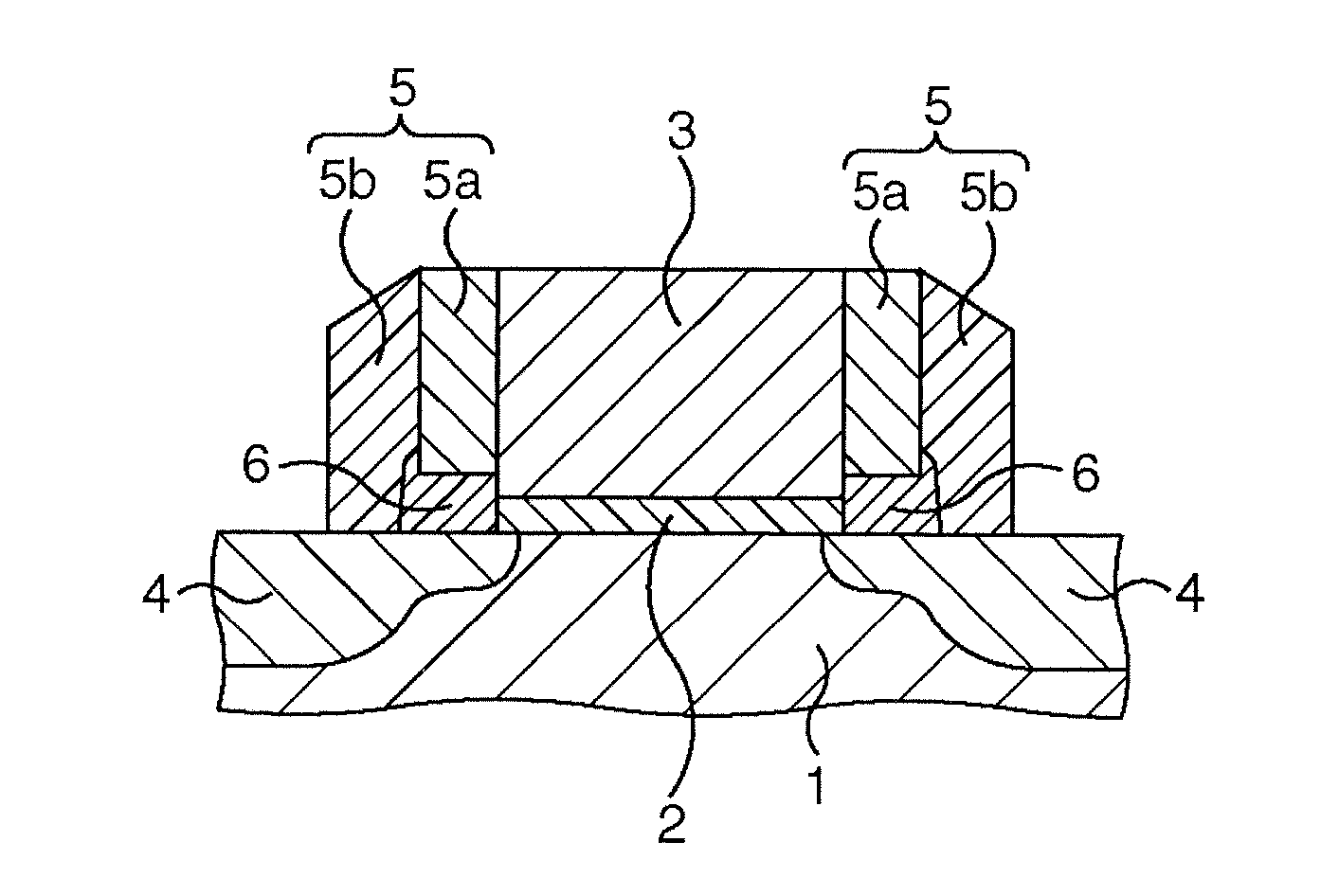
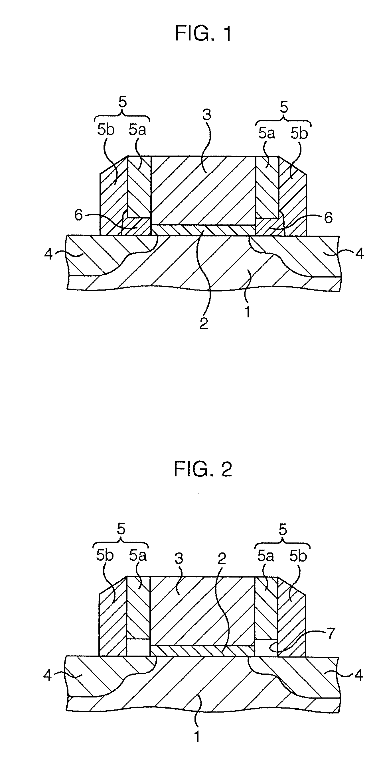
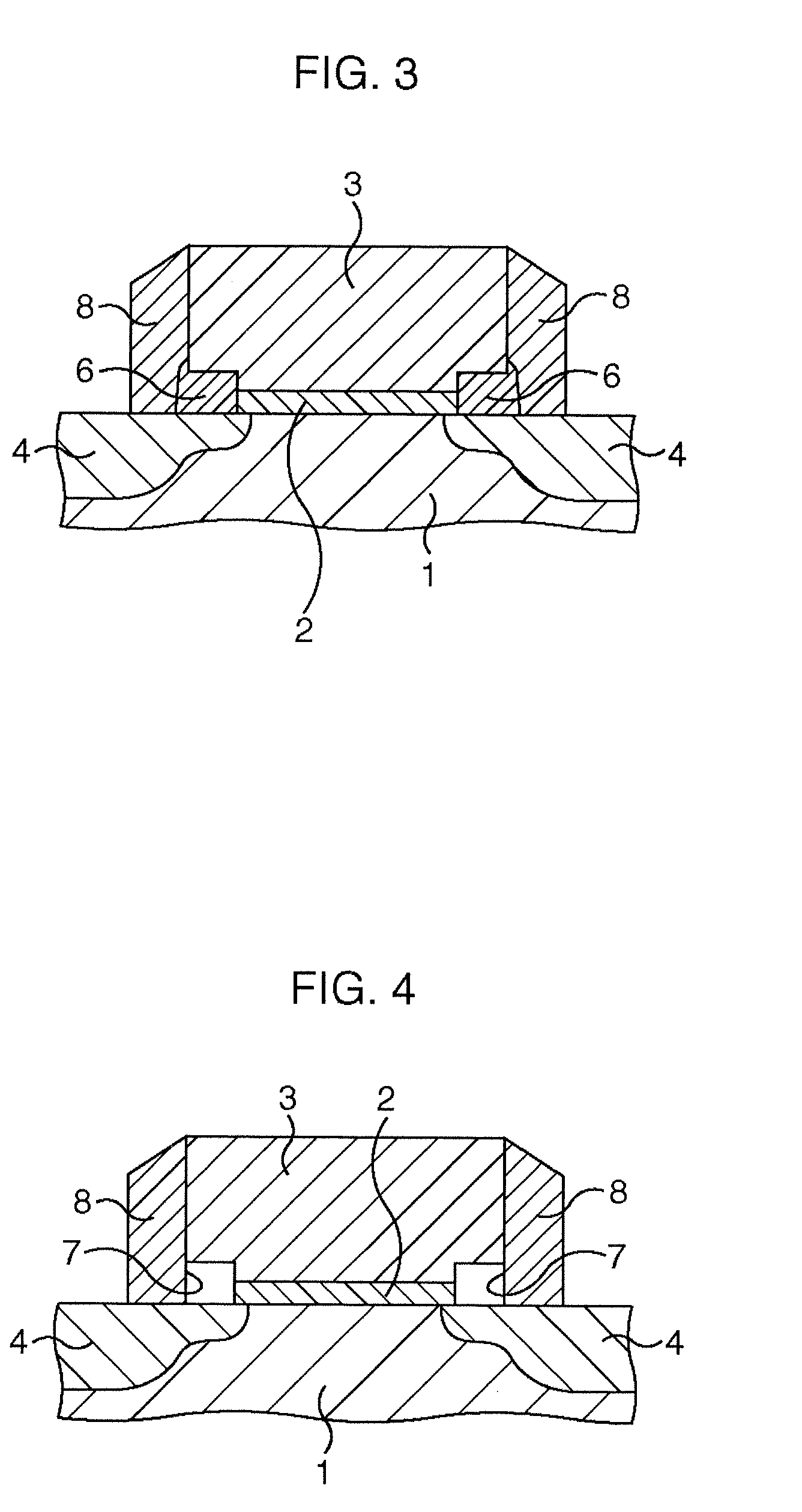
A MOS transistor has a gate electrode formed on a semiconductor substrate via a gate insulation film and a source and a drain formed on both sides of the gate electrode, wherein, with sidewall films each consisting of two layers (a thin first film and a second film for covering the first film), a lower part of the first film, that is, only a side lower portion of the gate electrode becomes a local low permittivity region to be filled in with a low permittivity material, and then the second film is formed to cover the low permittivity material.

Description

CROSS REFERENCE TO RELATED APPLICATIONS [0001] This application is based upon and claims the benefit of priority from the prior Japanese Patent Application No. 2002-255473, filed on Aug. 30, 2002, the entire contents of which are incorporated herein by reference. FIELD OF THE INVENTION [0002] The present invention relates to a semiconductor device such as a MOS transistor having a gate, a source, and a drain, and a method for manufacturing the same. DESCRIPTION OF THE RELATED ART [0003] Recently, along with progress in high integration and high performance for a semiconductor device, various demands for the semiconductor device have been still more increasing. Among them, strong demands are to make even thinner films of a gate insulation film and a sidewall insulation film. This causes to increase fringe capacitance, that is, parasitic capacitance generated mainly between a gate electrode and a semiconductor substrate, which is seen as a problem. As a conventional art to attempt red...

Claims


Application Information

Patent Timeline
IPC IPC(8): H01L29/423H01L21/28H01L21/336H01L29/49H01L29/78
CPCH01L21/28114H01L29/42376H01L29/4983H01L29/4991H01L29/6656H01L29/6659H01L29/7833H01L29/6653
Inventor TANAKA, TAKUJI
Owner FUJITSU LTD
Learn More