MIS semiconductor device and manufacturing method thereof

a semiconductor device and manufacturing method technology, applied in the direction of semiconductor devices, electrical devices, transistors, etc., can solve the problems of difficult to obtain a sufficient high driving current, increase of fringing capacitance of the gate, and deterioration of driving power, etc., to achieve suppressed short-channel effect, large driving current, and large driving current

Inactive Publication Date: 2006-02-21
RENESAS ELECTRONICS CORP
View PDF9 Cites 5 Cited by
  • Summary
  • Abstract
  • Description
  • Claims
  • Application Information

AI Technical Summary

Benefits of technology

[0014]As described above, with the conventional technologies, it is difficult to suppress the short-channel effect and to assure a large driving current at the same time.
[0015]It is thus an object of the present invention addressing the problems described above to provide a MIS semiconductor device that is excellent in that the short-channel effect can be suppressed and, at the same time, a large driving current can be assured, and to provide a method of manufacturing the MIS semiconductor device. Further, it is an object of the present invention to provide a MIS semiconductor device and its manufacturing method which realize a reduction of the fringing capacitance of the gate and speeding-up of the signal delay.

Problems solved by technology

Thus, the resistance of a source / drain parasitic resistance increases, giving rise to a demerit of a deteriorating driving power.
Thus, even if a material having a high dielectric constant is used for making the first side-wall spacer, it is difficult to obtain a sufficient high driving current.
Furthermore, if all materials used for making the first side-wall spacer have a high dielectric constant as described above, the fringing capacitance of the gate will increase, raising a problem of an extremely long signal delay.

Method used


Image

  • MIS semiconductor device and manufacturing method thereof
  • MIS semiconductor device and manufacturing method thereof
  • MIS semiconductor device and manufacturing method thereof

Examples


second embodiment

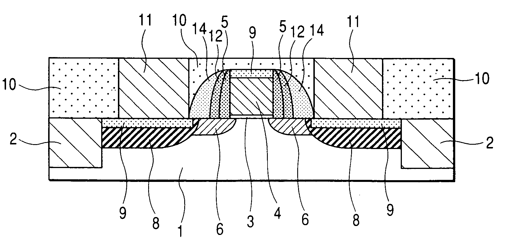
[0069]Next, a second embodiment is explained by referring to FIG. 6. FIG. 6 is a complete cross-sectional diagram showing a MIS field-effect transistor for a case in which it is necessary to set the width of a side-wall spacer at a value of more than or equal to 15 nm.

first embodiment

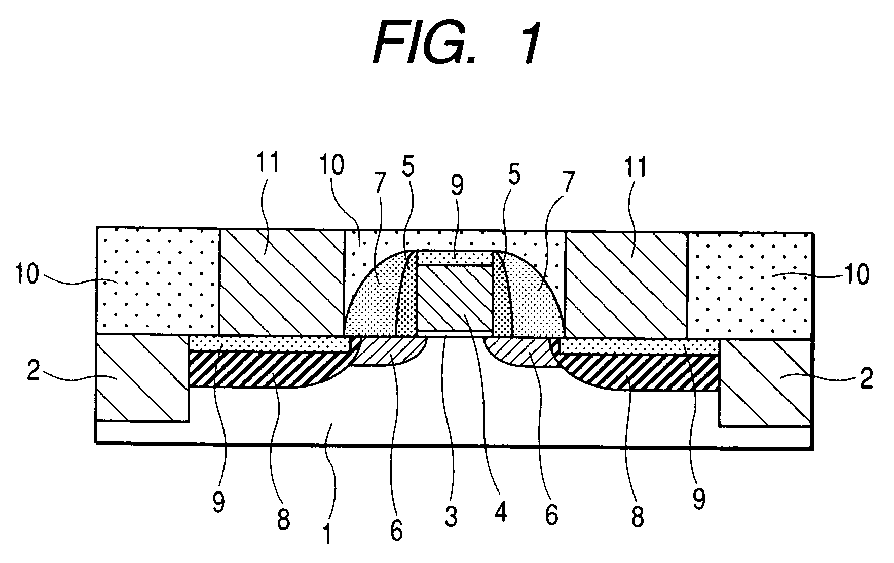
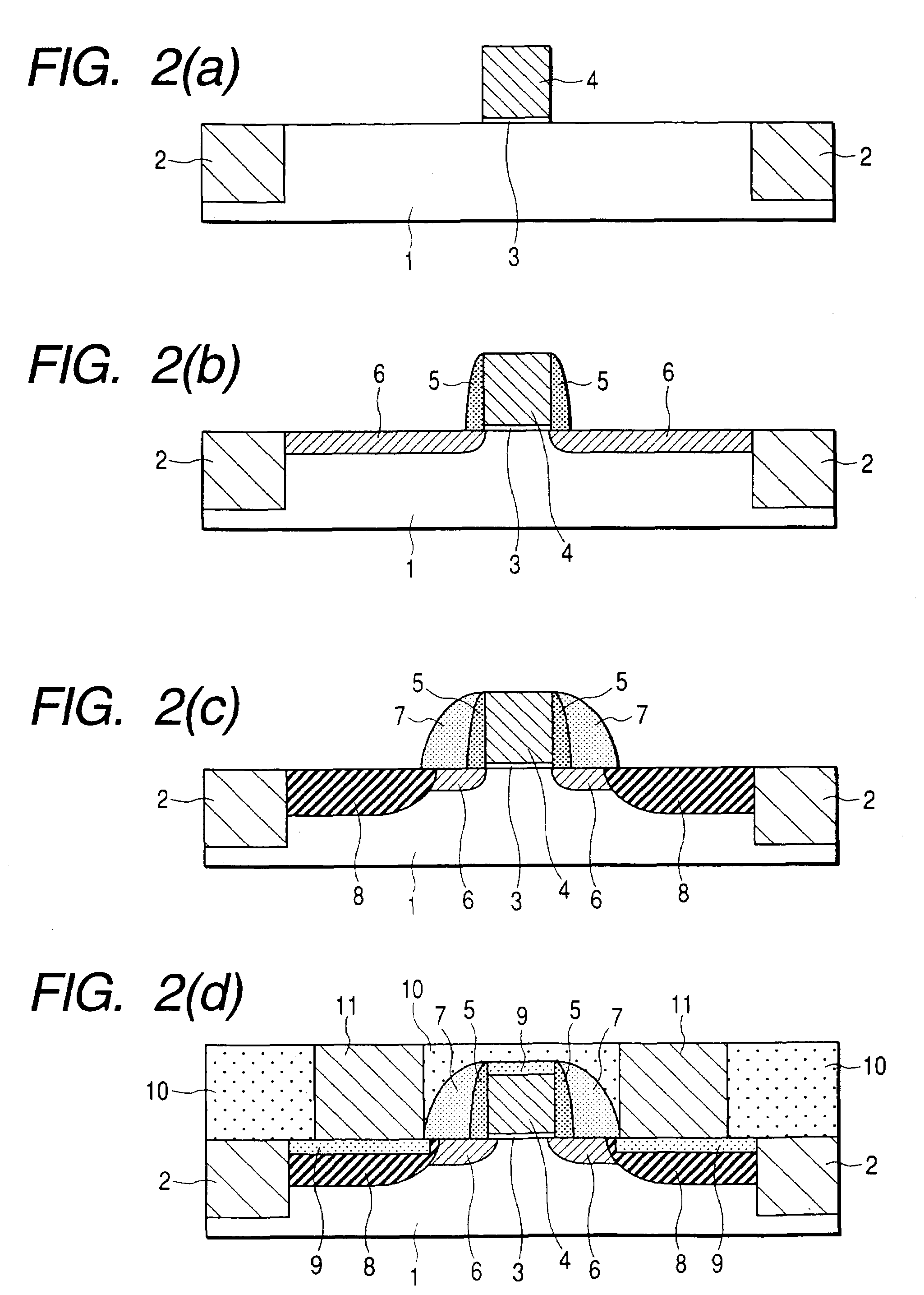
[0070]Much like the first embodiment explained earlier, a gate dielectric 3 and a gate electrode 4 made of poly-silicon are formed on a silicon substrate 1. Then, a dielectric is deposited on the silicon substrate 1 by adopting typically the CVD technique. The dielectric whose dielectric constant is greater than a silicon-oxide film is then etched back to leave a first side-wall spacer 5 having a width typically in the range 5 nm to 15 nm on the side wall of the gate electrode 4. Examples of such a dielectric are a silicon-nitride film, a silicon film, an aluminum oxide film, a tantalum oxide film, a titanium oxide film, a zirconium dioxide film and a hafnium oxide film. At that time, in order to assure reliability of the device, light oxidation is carried out at a temperature of typically 650° C. prior to the process to stack the first side-wall spacer 5 on the silicon substrate 1 in order to cover the surface of the silicon substrate 1 and the surface of the gate electrode 4 with ...

fourth embodiment

[0079]Even in the case of the fourth embodiment employing the first thin film 13 and the second film 14 as described above, the short-channel effect of the transistor can be suppressed and the driving current of the transistor can be increased.

[0080]FIG. 9 is a complete cross-sectional diagram showing a MIS field-effect transistor implemented by a fifth embodiment of the present invention. The fifth embodiment is an embodiment wherein an N-channel transistor and a P-channel transistor are fabricated on the same substrate in accordance with the present invention. The fifth embodiment shown in FIG. 9 implements a method of manufacturing a semiconductor device allowing the effective gate length of the N-channel transistor and that of the P-channel transistor to be set independently with each other by combining the first embodiment described earlier with the conventional manufacturing method.

[0081]After a P well area 20, an N well area 21 and an element separation field oxide film 2 are...


PUM


Abstract

By suppressing a short-channel effect of a MIS field-effect transistor and reducing a fringing capacitance of a gate, a signal delay in the transistor can be shortened. The MIS field-effect transistor is formed d by forming a side-wall spacer from a dielectric having a large dielectric constant and then forming an impurity diffusion layer area with the side-wall spacer used as an introduction end in an ion implantation process to introduce impurities. In this case, the side wall of the side-wall spacer having the large dielectric constant has an optimum film thickness in the range from 5 nm to 15 nm, which is required for achieving a large driving current. On the other hand, a side-wall spacer on an outer side is made of a silicon-dioxide film, which is a dielectric having a small dielectric constant.

Description

[0001]This is a continuation application of U.S. Ser. No. 10 / 372,329, filed Feb. 25, 2003 now U.S. Pat. No. 6,744,099.BACKGROUND OF THE INVENTION[0002]1. Field of the Invention[0003]In general, the present invention relates to a semiconductor device and a manufacturing method thereof. More particularly, the present invention relates to enhancement of an operating current of a super-miniaturized MIS semiconductor device and super enhancement of an operating speed of the MIS semiconductor device.[0004]2. Description of the Related Art[0005]Enhancement of performance of an insulated-gate field-effect transistor or, in particular, a MIS field-effect transistor (hereinafter, simply abbreviated to MISFET) employed in a super-density semiconductor device is based on a scaling law and has been successful. The success of the enhancement of an insulated-gate field-effect transistor's performance is attributed to a decrease in applied power-supply voltage, a decrease in transistor area and min...

Claims


Application Information

Patent Timeline
Patent Type & Authority Patents(United States)
IPC IPC(8): H01L21/336H01L27/092H01L21/8238H01L29/49H01L29/78
CPCH01L21/823864H01L29/4983H01L29/6656H01L29/6659Y10S257/90H01L29/665H01L21/18
Inventor TSUCHIYA, RYUTAHORIUCHI, MASATADA
Owner RENESAS ELECTRONICS CORP
Why Eureka
Try Eureka