
Thin Polysilicon For Lower Off-Capacitance Of A Radio Frequency (RF) Silicon-On-Insulator (SOI) Switch Field Effect Transistor (FET)

a technology of cmos transistor and polysilicon, which is applied in the direction of transistors, solid-state devices, basic electric elements, etc., can solve the problems of low operating voltage and unsuitable for implementing rf switches, and achieve the effects of reducing contact-to-polysilicon capacitance, reducing metal one, and reducing fringing capacitan

Inactive Publication Date: 2018-09-20
NEWPORT FAB
View PDF6 Cites 0 Cited by
  • Summary
  • Abstract
  • Description
  • Claims
  • Application Information

AI Technical Summary

Benefits of technology

The patent describes a new way of making semiconductor components called SOI CMOS transistors. These transistors have a thin layer of polysilicon that acts as a gate, which helps reduce capacitance and lower the off-capacitance of the associated RF switch. This results in a more efficient RF switch that has lower power consumption and higher performance. In addition, the thin gate layer also inhibits a depletion effect that can occur in some materials, which leads to lower on-resistance.

Problems solved by technology

Note that transistors fabricated using more advanced process nodes (e.g., a 0.13 micron process node) have lower operating voltages (e.g., 1.2 Volts or lower), and are typically not suitable for implementing an RF switch.

Method used


Image

  • Thin Polysilicon For Lower Off-Capacitance Of A Radio Frequency (RF) Silicon-On-Insulator (SOI) Switch Field Effect Transistor (FET)
  • Thin Polysilicon For Lower Off-Capacitance Of A Radio Frequency (RF) Silicon-On-Insulator (SOI) Switch Field Effect Transistor (FET)
  • Thin Polysilicon For Lower Off-Capacitance Of A Radio Frequency (RF) Silicon-On-Insulator (SOI) Switch Field Effect Transistor (FET)

Examples


Embodiment Construction

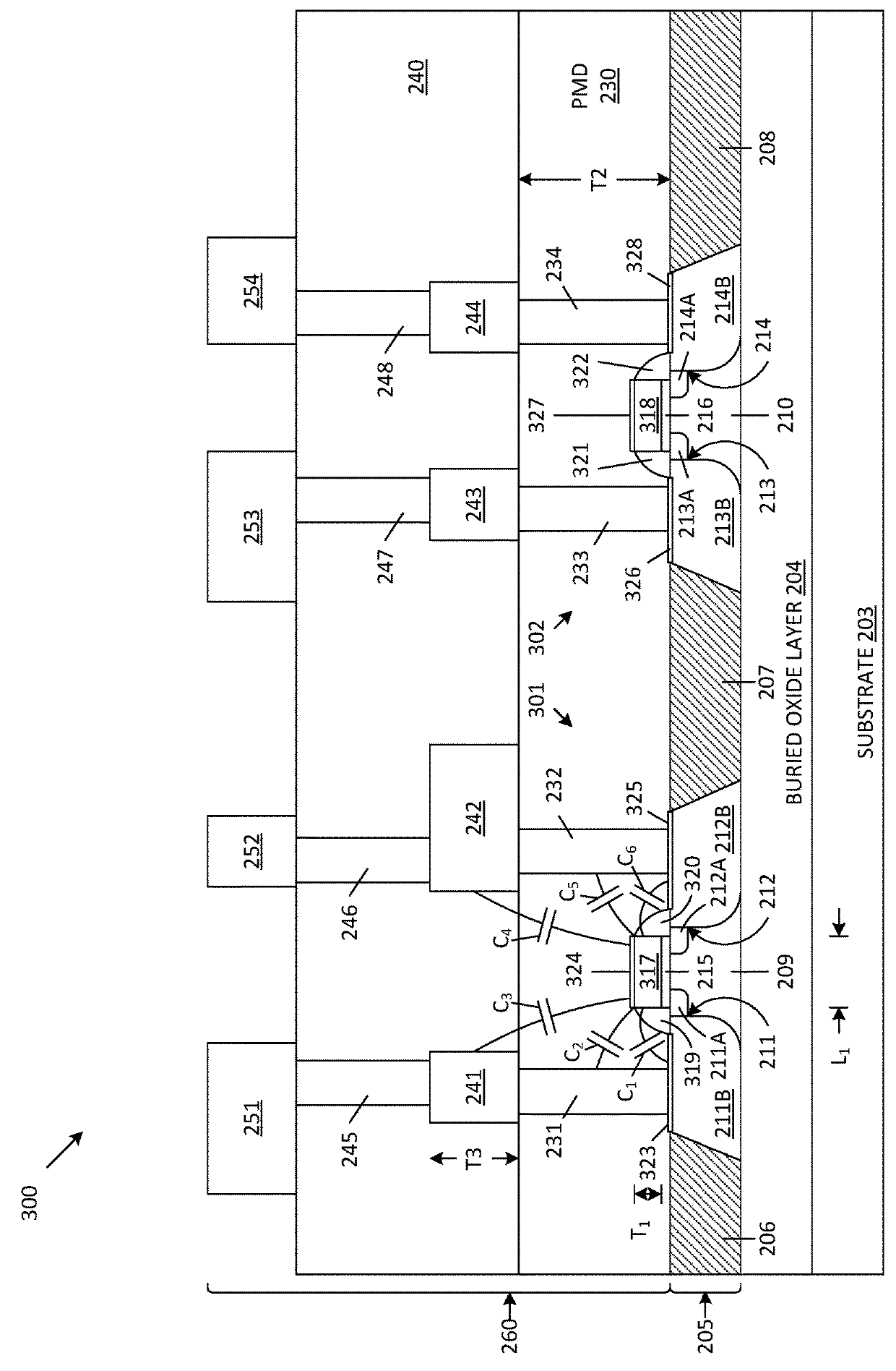
[0023]In general, the present invention includes an RF switch that includes a plurality of n-channel SOI CMOS transistors connected in series. The n-channel SOI CMOS transistors are fabricated in accordance with a conventional SOI CMOS process node, with the exception of the formation of the polysilicon gate layer. In accordance with the present invention, the polysilicon gate layer is thinner than a polysilicon layer typically associated with the conventional SOI CMOS process node. For example, n-channel SOI CMOS transistors may be fabricated substantially in accordance with a 0.18 micron SOI CMOS process node. The polysilicon gate layer of a 0.18 SOI CMOS process node typically has thicknesses of about 2000 Angstroms. However, in accordance with the present invention, the polysilicon gate layer is fabricated to have a thickness less than about 1450 Angstroms. For example, the polysilicon gate layer may have a thickness in the range of about 1350 to 1150 Angstroms. In another embod...


PUM


Abstract

A radio frequency (RF) switch includes a plurality of series-connected silicon-on-insulator (SOI) CMOS transistors fabricated in accordance with a semiconductor process having a first minimum line width (e.g., 0.18 microns). While the semiconductor process conventionally implements a polysilicon gate layer having a first thickness (e.g., 2000 Angstroms), each of the plurality of SOI CMOS transistors is fabricated with a polysilicon gate electrode having a second thickness, which is less than the first thickness. The reduced thickness of the polysilicon gate electrodes of the SOI CMOS transistors reduces the on-resistance and the off-capacitance of the associated RF switch.

Description

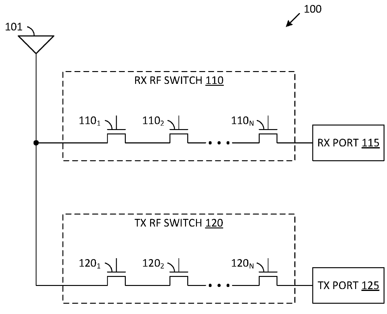
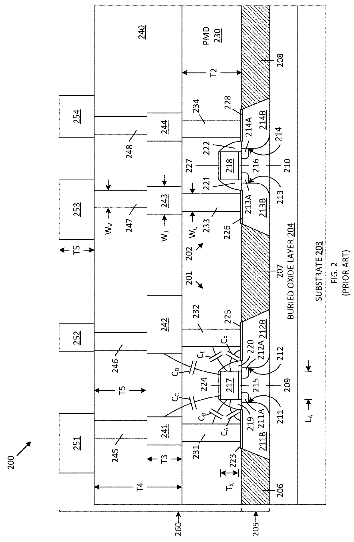
FIELD OF THE INVENTION[0001]The present invention relates to a radio frequency (RF) switch including a plurality of silicon-on-insulator (SOI) CMOS transistors.RELATED ART[0002]FIG. 1 is a circuit diagram of a conventional radio frequency (RF) circuit 100, including an antenna 101, an RF receiver switch 110, an RF receiver port 115, an RF transmitter switch 120 and an RF transmitter port 125. RF receiver switch 110 includes a plurality of high-voltage field effect transistors (FETs) 1101-110N, which are connected in series (in a stack). The stack of high voltage FETs 1101-110N is controlled to route RF signals from antenna 101 to receive port 115. Similarly, RF transmitter switch 120 includes a stack of high-voltage FETs 1201-120N, which are controlled to route RF signals from transmit port 125 to antenna 101. As used herein, an RF signal is defined as a signal having a frequency in the range of about 10 kHz to 50 GHz. The FETs used in the switch branch stack are large, typically 1-...

Claims


Application Information

Patent Timeline
Patent Type & Authority Applications(United States)
IPC IPC(8): H01L27/12H01L29/49H01L29/423H01L21/84H01L23/528H01L27/092H01Q1/22
CPCH01L27/1203H01L29/4916H01L29/42376H01Q1/2283H01L23/5283H01L27/092H01L21/84H01L29/42384H01L29/7833
Inventor KANAWATI, RODA
Owner NEWPORT FAB
Learn More