Power metal oxide semiconductor transistor layout with lower output resistance and high current limit

a technology of semiconductor transistors and layouts, applied in semiconductor devices, semiconductor/solid-state device details, electrical apparatus, etc., can solve the problems of severe voltage drop at metal connections, limited line width of source and drain metal connections, and limited length of source and drain connections, etc., to achieve low output resistance and high current limit

Active Publication Date: 2006-11-07
RICHTEK TECH
View PDF7 Cites 40 Cited by
  • Summary
  • Abstract
  • Description
  • Claims
  • Application Information

AI Technical Summary

Benefits of technology

[0008]It is therefore an object of the invention to provide a power metal oxide semiconductor transistor layout with a lower output resistance and a high current limit.
[0009]It is another object of this invention to provide a power metal oxide semiconductor transistor layout with a high uniformity of current, low Rds_on, much less power loss, an actual line density two times larger than that of conventional layouts and a strengthened resistance to electron migration.
[0010]It is a further object of this invention to provide power metal oxide semiconductor transistor layout with a high package density.

Problems solved by technology

However, the long source and drain connection results in some drawbacks such as a severe voltage drop at metal connection.
Thus, the line width of source and drain metal connection is limited.
The length of line of source and drain connection is also limited by electron migration especially for limited line width.
So, it is a dilemma to achieve a power MOS transistor with high current and high packing density layout.
The conventional MOSFET current driver layout is prone to have shorts or defects.
First of all, the long source and drain connection would result in severe voltage drop at metal connection.
Moreover, the line width of source and drain metal connection is also limited by electron migration.
First of all, the line width of source and drain metal connection line is limited due to the source and drain connected by high resistance diffusion layer.
Moreover, the line length of source and drain connection is also limited by electron migration.

Method used


Image

  • Power metal oxide semiconductor transistor layout with lower output resistance and high current limit
  • Power metal oxide semiconductor transistor layout with lower output resistance and high current limit
  • Power metal oxide semiconductor transistor layout with lower output resistance and high current limit

Examples


Embodiment Construction

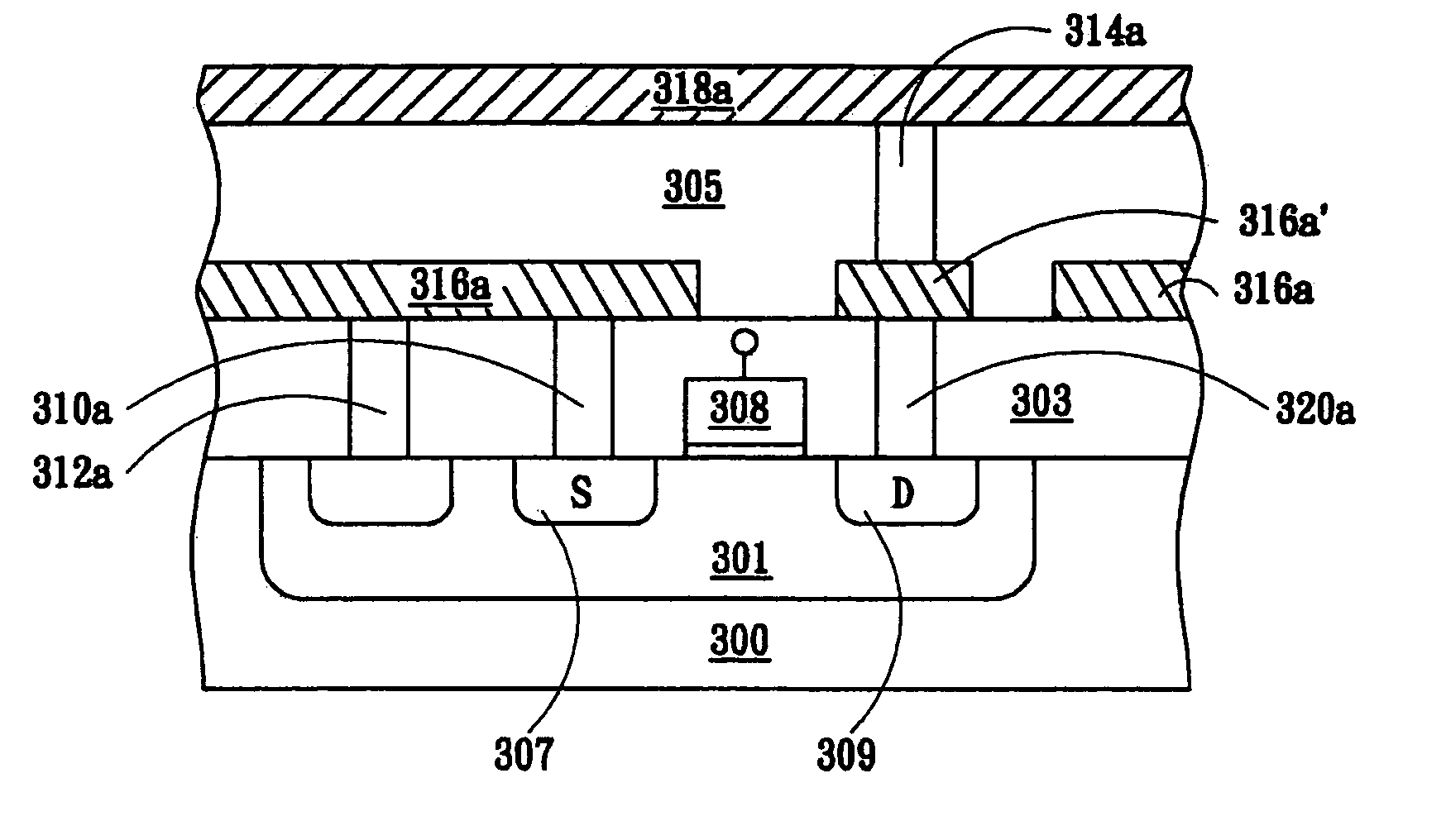
[0037]Referring to FIG. 3, a schematic diagram of one embodiment of a power metal oxide semiconductor (MOS) transistor layout of the invention is shown. The power MOS transistor layout comprises areas 302, 304 and 306. The power MOS transistor layout of the invention uses a network of conductive lead line and a conductive plane as the interconnection between the source and drain of the power MOS transistor layout. Referring to FIG. 3A, a top view of a portion of the area 302 is shown. The power MOS transistor layout comprises a polysilicon gate 308 with a square lattice pattern, source regions and drain regions. Each source region is laid to be surrounded by four drain regions and each drain region is laid in a similar manner. In the area 302, the power MOS transistor layout uses a network of conductive lead line 316a as the interconnection of the source regions and the well pickup contacts and a conductive plane 318a as the interconnection of the drain regions. The network of condu...


PUM


Abstract

A power metal oxide semiconductor transistor layout is disclosed. The power metal oxide semiconductor transistor layout uses network of conductive lead line as a connection or a network connection to connect source and drain regions thereby achieves advantages of a high uniformity of current, low Rds_on, much less power loss, an actual line density two times larger than that of conventional layouts and a strengthened resistance to electron migration.

Description

BACKGROUND OF THE INVENTION[0001]1. Field of the Invention[0002]The present invention relates to a power metal oxide semiconductor transistor layout, and more particularly to a power metal oxide semiconductor transistor layout with a lower output resistance and a high current limit.[0003]2. Description of the Related Art[0004]Metal oxide semiconductor (MOS) transistors with very large line width are widely used as power switch of power management application. However, the long source and drain connection results in some drawbacks such as a severe voltage drop at metal connection. Moreover, the cell pitch of power device must be as small as possible so as to increase packing density. Thus, the line width of source and drain metal connection is limited. The length of line of source and drain connection is also limited by electron migration especially for limited line width. So, it is a dilemma to achieve a power MOS transistor with high current and high packing density layout.[0005]Re...

Claims


Application Information

Patent Timeline
Patent Type & Authority Patents(United States)
IPC IPC(8): H01L29/94
CPCH01L23/4824H01L29/41758H01L29/4238H01L29/78H01L2924/0002H01L2924/00
Inventor SU, HUNG-DERHUANG, CHUN-YENPAI, CHUNG-LUNGLIU, JING-MENG
Owner RICHTEK TECH
Why Eureka
Try Eureka