Semiconductor integrated circuit including operation test circuit and operation test method thereof

a technology of integrated circuits and test circuits, applied in the direction of instruments, error detection/correction, solid-state devices, etc., can solve the problems of inability to cope with a case, the difficulty of operation test of lsi on the assumption of actual operation

Inactive Publication Date: 2006-11-07
KK TOSHIBA
View PDF5 Cites 4 Cited by
  • Summary
  • Abstract
  • Description
  • Claims
  • Application Information

AI Technical Summary

Benefits of technology

[0058]controlling the phase control circuit, the first selector, the second selector, the evaluation data generating circuit, and the expected value comparison circuit, and sequentially shifting a phase of the second clock signal so that a phase difference between the first clock signal and the second clock signal increases until the output data and the expected value become non-coincident when the output data and the expected value coincide in the expected value comparison circuit.

Problems solved by technology

Recently, however, the operation performance of the LSI has achieved further development, and consequently the frequency of the clock signal supplied from the external LSI tester and an operating frequency in an actual operation become widely different, whereby the operation test of the LSI on the assumption of the actual operation is becoming more and more difficult.
Moreover, in the aforementioned related operation test circuit, only one path to be evaluated is fixed by positions where two-phase synchronous flip-flops are provided, which cannot cope with a case where the path to be evaluated needs to be changed in the operation test.

Method used


Image

  • Semiconductor integrated circuit including operation test circuit and operation test method thereof
  • Semiconductor integrated circuit including operation test circuit and operation test method thereof
  • Semiconductor integrated circuit including operation test circuit and operation test method thereof

Examples


first embodiment

[0070](First Embodiment)

[0071]Hereinafter, a first embodiment of a semiconductor integrated circuit including an operation test circuit and an operation test method will be explained with reference to FIG. 1 to FIG. 4.

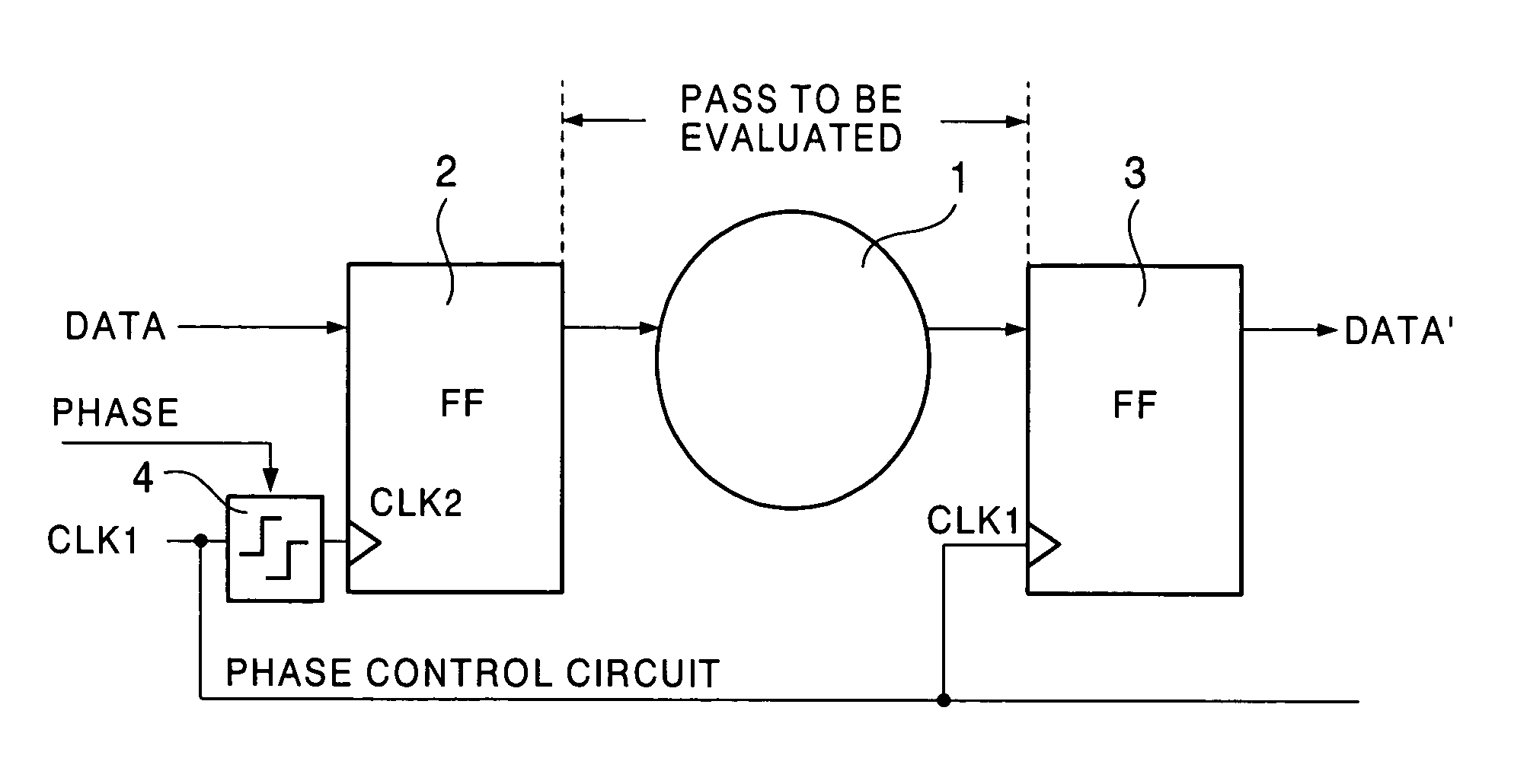
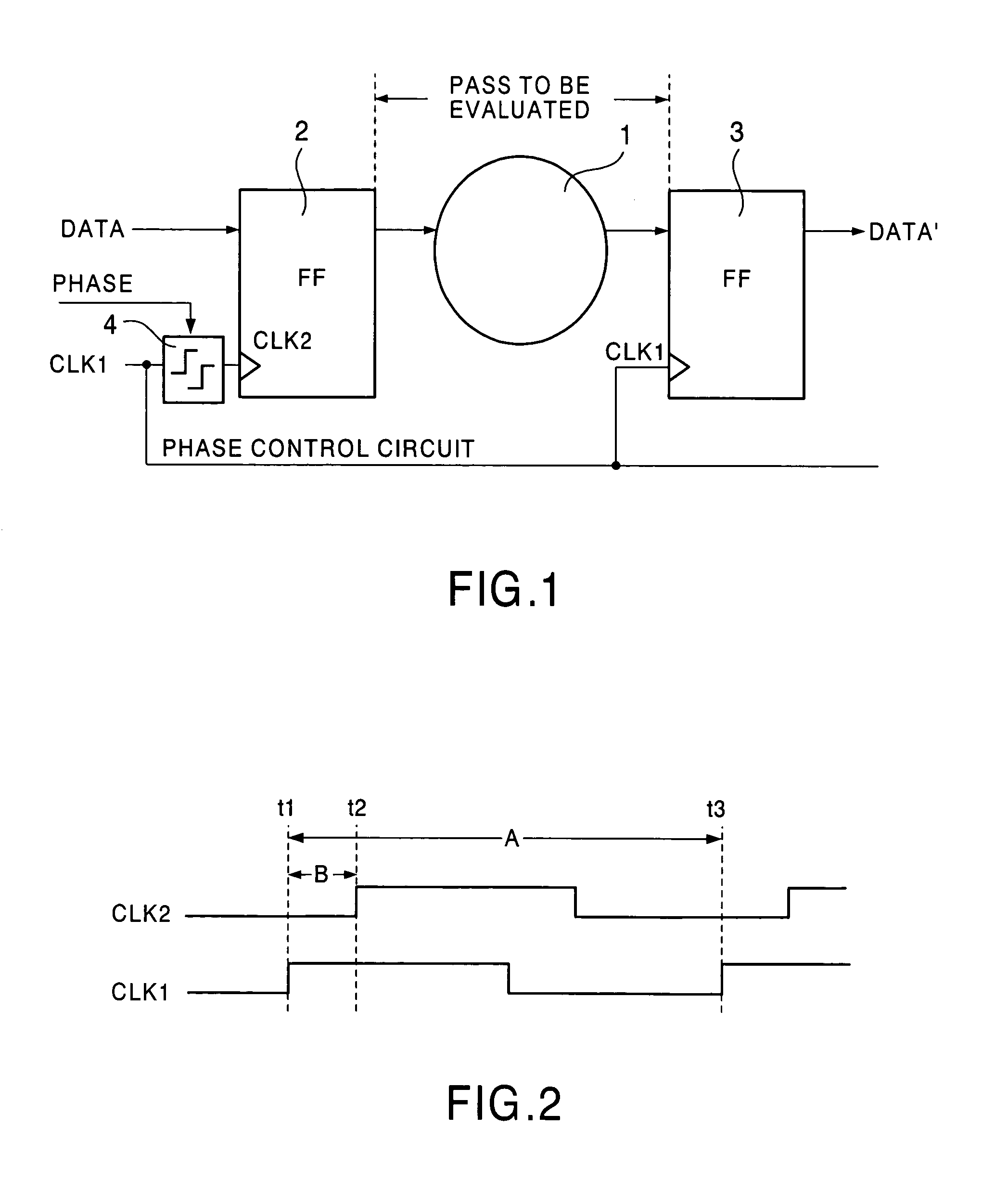
[0072]First, a semiconductor integrated circuit including an operation test circuit according to this embodiment will be explained with reference to FIG. 1 to FIG. 3. FIG. 1 schematically shows the configuration of the semiconductor integrated circuit including the operation test circuit according to this embodiment.

[0073]A first and second flip-flops 2 and 3 are provided at both ends of a circuit under test 1 on which an operation test is to be performed. Evolution data DATA is inputted to the circuit under test 1 via the first flop-flop 2, and output data DATA′ is outputted via the second flip-flop 3.

[0074]A fist clock signal CLK1 for flip-flop control is supplied to the second flip-flop 3, and a second clock signal CLK2, which is obtained by the first clock signal C...

second embodiment

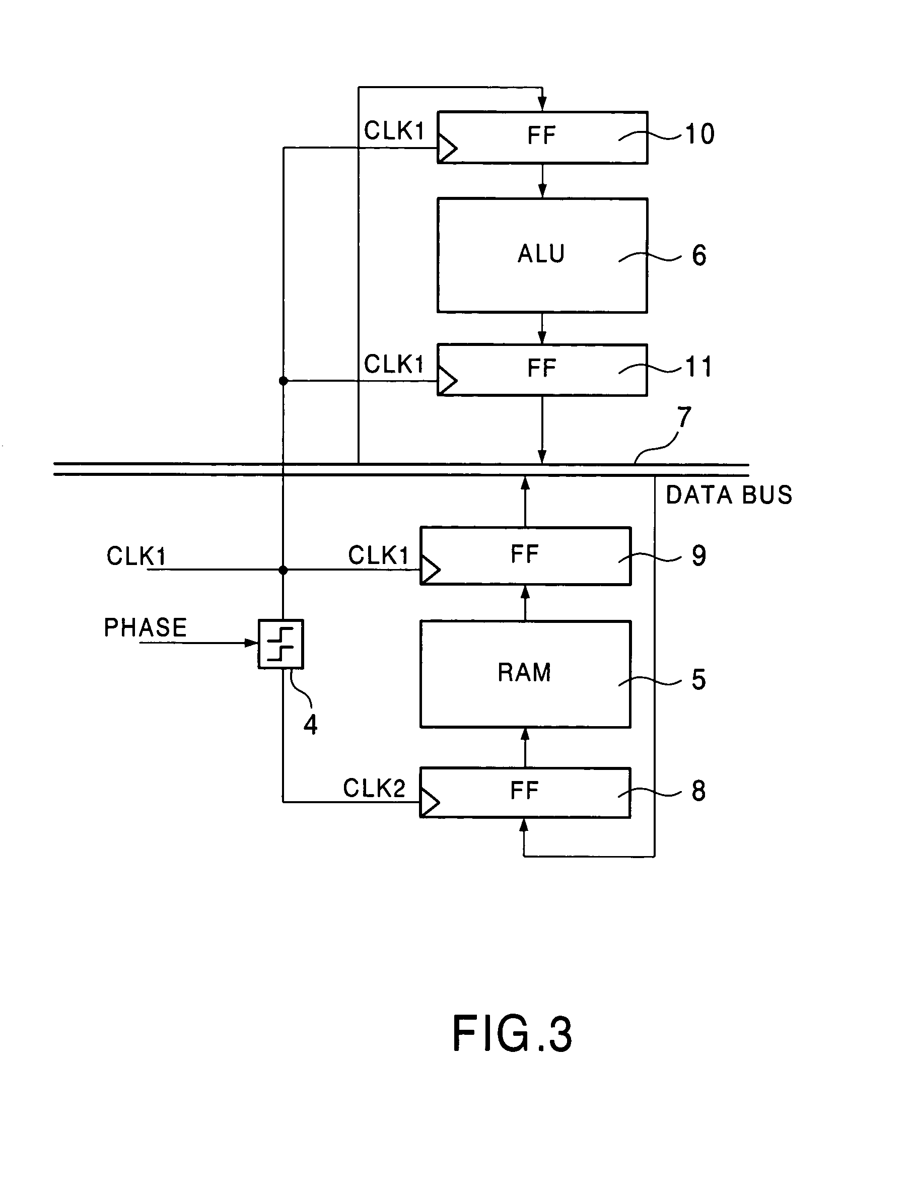
[0099](Second Embodiment)

[0100]Hereinafter, a second embodiment of the semiconductor integrated circuit including the operation test circuit and an operation test method will be explained with reference to FIG. 5 to FIG. 7.

[0101]First, a semiconductor integrated circuit including an operation test circuit according to this embodiment will be explained with reference to FIG. 5 and FIG 6. FIG. 5 schematically shows the configuration of the semiconductor integrated circuit including the operation test circuit according to this embodiment. Incidentally, the same numerals and symbols as in FIG. 1 are used to designate components corresponding to those in FIG. 1, so that the explanation thereof are omitted.

[0102]A clock signal line is branched to provide two system clock signals, the first clock signal CLK1 used as a system clock and the second clock signal CLK2 whose phase is shifted by the phase control circuit 4. A first selector 12 and a second selector 13 are provided for the first f...

third embodiment

[0124](Third Embodiment)

[0125]Hereinafter, a third embodiment of the semiconductor integrated circuit including the operation test circuit will be explained with reference to FIG. 8 to FIG. 9.

[0126]FIG. 8 schematically shows the configuration of a semiconductor integrated circuit including an operation test circuit according to the third embodiment. It is noted that since the configuration of the operation test circuit according to this embodiment is partly in common with the configurations of the operation test circuits according to the first and second embodiments, the same numerals and symbols are used to designate components corresponding to those in FIG. 1 and FIG. 5, and the explanation thereof is omitted.

[0127]An evaluation data generating circuit 18 generates the evaluation data DATA and supplies it to the first flip-flop 2, an output of the circuit under test 1 outputted via the second flip-flop 3 by the input of the evaluation data DATA is supplied to an expected value com...


PUM


Abstract

A semiconductor integrated circuit disclosed herein comprising: a phase control circuit which shifts a phase of a first clock signal based on a phase control signal and outputs a second clock signal; a first flip-flop to which one of the first clock signal and the second clock signal is inputted as a first operation clock signal, and which outputs evaluation data; a circuit under test which performs a predetermined process based on the evaluation data and outputs a result of the process as output data; and a second flip-flop to which the other of the first clock signal and the second clock signal is inputted as a second operation clock signal and the output data is inputted, and which outputs the output data inputted from the circuit under test.

Description

CROSS REFERENCE TO RELATED APPLICATION[0001]This application claims benefit of priority under 35 U.S.C. §119 to Japanese Patent Application No. 2003-001741, filed on Jan. 8, 2003, the entire contents of which are incorporated by reference herein.BACKGROUND OF THE INVENTION[0002]1. Field of the Invention[0003]The present invention relates to a semiconductor integrated circuit including an operation test circuit and an operation test method thereof.[0004]2. Related Background Art[0005]Hitherto, an operation test of an semiconductor integrate circuit (hereinafter referred to as an LSI) has been generally performed by supplying an operation test clock signal to the LSI by an external LSI tester.[0006]Recently, however, the operation performance of the LSI has achieved further development, and consequently the frequency of the clock signal supplied from the external LSI tester and an operating frequency in an actual operation become widely different, whereby the operation test of the LSI...

Claims


Application Information

Patent Timeline
Patent Type & Authority Patents(United States)
IPC IPC(8): G01R31/28G06F11/00G01R31/317G01R31/3183H01L21/822H01L27/04
CPCG01R31/31727
Inventor TANAKA, YOSHIYUKIOJIMA, YOSHINARI
Owner KK TOSHIBA
Why Eureka
Try Eureka