Method and apparatus for phase-matched optical and RF wave propagations for semiconductor-based mzm modulators

a technology of phase-matched optical and rf wave propagation, which is applied in the field of optical modulators, can solve the problems of high optical loss and high vpi, limit to the application and high power consumption of the modulator driver

Active Publication Date: 2018-07-19
NEOPHOTONICS CORP
View PDF2 Cites 1 Cited by
  • Summary
  • Abstract
  • Description
  • Claims
  • Application Information

AI Technical Summary

Benefits of technology

[0006]In a further aspect, the invention pertains to an optical modulator comprising a semiconductor-based optical waveguide and a RF waveguide configured to form an coupling region over which electro-optical coupling occurs to modulate an optical signal within the semiconductor-based optical waveguide, wherein the semiconductor-based optical waveguide comprises a p-n junction formed according to corresponding doping of the semiconductor along a cross section through the optical waveguide perpendicular to a light propagation direction, in which the doping varies at one or more compensation sections along the semiconductor-based optical waveguide to reduce accumulated phase difference between an optical transmission in the semiconductor-based optical waveguide and an RF signal in the RF waveguide.

Problems solved by technology

Silicon-on-insulator (SOI) platform, which can be used to make optical waveguide, has appeared as the emerging technology for optoelectronics devices including MZM modulators since SOI fabrication infrastructure is compatible with CMOS technology and is suitable for photonic integration; however, the most promising technology for SOI based optical modulation, which uses carrier depletion through doped P-N junction, suffers high optical loss and high Vpi, where Vpi is defined as the voltage required to generate Pi phase shift on MZM arms.
High Vpi requires high driver voltage and thus high power consumption for modulator drivers, which limit to their applications where low power consumptions are required.

Method used


Image

  • Method and apparatus for phase-matched optical and RF wave propagations for semiconductor-based mzm modulators
  • Method and apparatus for phase-matched optical and RF wave propagations for semiconductor-based mzm modulators
  • Method and apparatus for phase-matched optical and RF wave propagations for semiconductor-based mzm modulators

Examples


Embodiment Construction

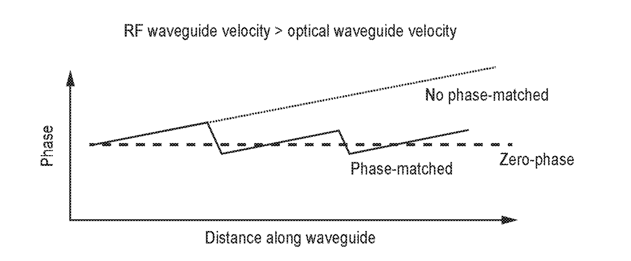
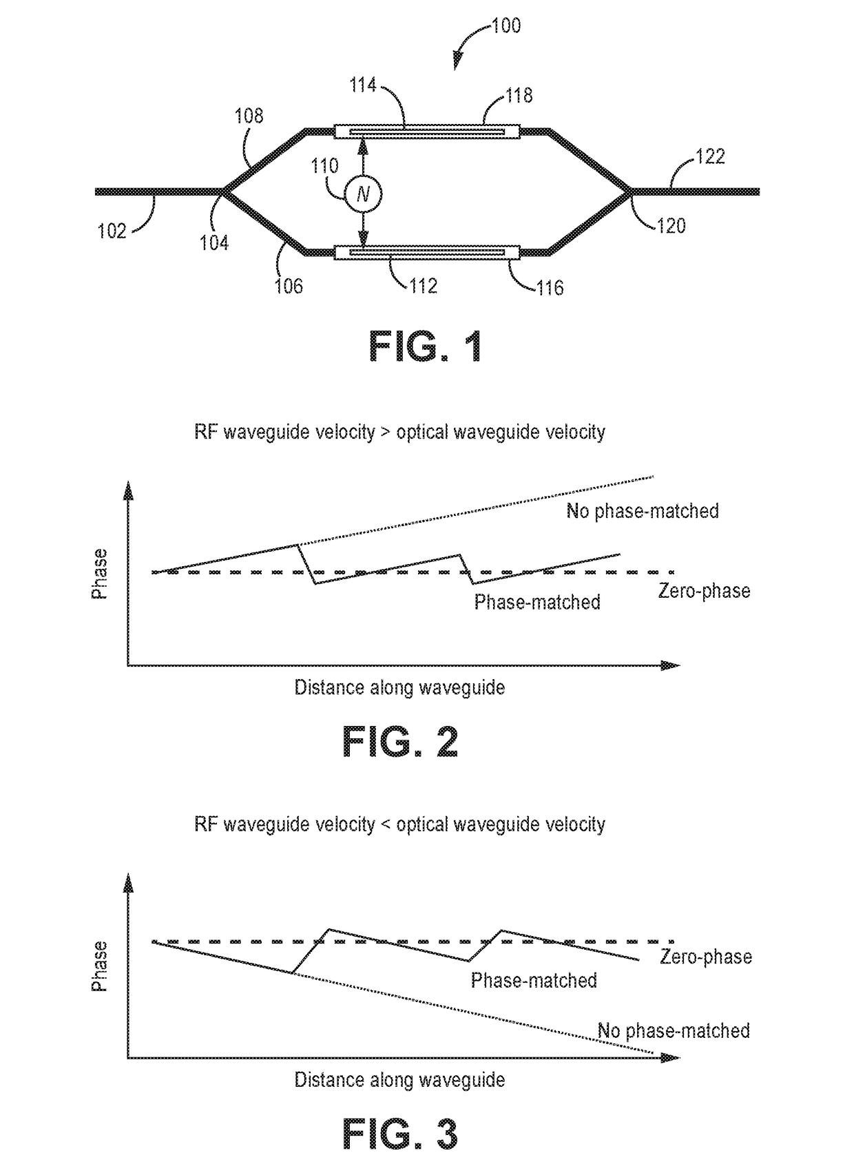
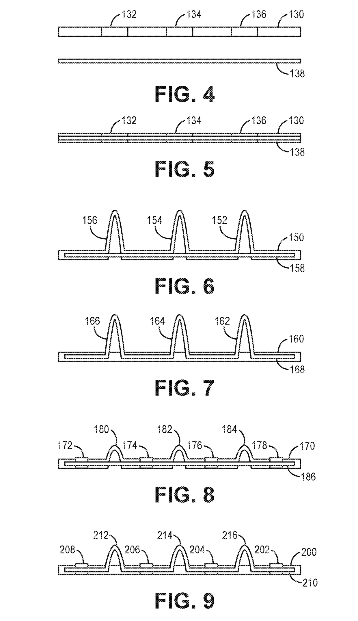
[0032]RF driven optical modulator structures are described that can compensate for phase misalignment between an RF signal and an optical signal within a traveling wave electro-optical coupling structure with a Mach-Zehnder modulator (MZM) design. The modifications to provide phase compensation are particularly applicable to semiconductor based optical waveguides, especially silicon-based optical waveguides. As used herein, silicon-based refers to elemental silicon materials that can be doped and does not refer to silicon dioxide based glass waveguides. To adjust the relative phases of the optical propagation and RF propagation through the coupled waveguides of the traveling wave structure, in some embodiments, either the optical waveguide or the RF waveguide in a compensation section can be looped out of a coupling configuration to phase shift the propagations relative to each other for better phase alignment upon rejoining of the two signals. In additional or alternative embodimen...


PUM

PropertyMeasurementUnit
sizesaaaaaaaaaa
lengthsaaaaaaaaaa
semiconductoraaaaaaaaaa

Abstract

Optical modulators with semiconductor based optical waveguides interacting with an RF waveguide in a traveling wave structure. The semiconductor optical waveguide generally comprise a p-n junction along the waveguide. To reduce the phase walk-off between the optical signal and the RF signal, the traveling wave structure can comprise one or more compensation sections where the phase walk-off is reversed. The compensation sections can comprise a change in dopant concentrations, extra length for the optical waveguide and/or extra length for the RF waveguide. Corresponding methods are described.

Description

CROSS REFERENCE TO RELATED APPLICATIONS[0001]This application claims priority to copending U.S. provisional patent application 62 / 447,521 to Zhou et al. filed on Jan. 18, 2017, entitled “Method and Apparatus for Phase-Matched Optical and RF Wave Propagations for High Speed High Efficiency Linear MZM Modulators,” incorporated herein by reference.FIELD OF THE INVENTION[0002]The invention relates to optical modulators comprising a semiconductor optical waveguide interfaced with RF waveguides in which electro-optical coupling provides a modulation to the optical signal. The invention further relates to waveguide designs to decrease phase shifts between propagating electrical signals and optical intensity propagating through the respective waveguides.BACKGROUND OF THE INVENTION[0003]A traveling wave structure is widely used in high speed linear modulators with Mach-Zehnder modulator (MZM) structures with traditional material platforms such as LiNbO3 and InP. Silicon-on-insulator (SOI) pl...

Claims


Application Information

Patent Timeline
Patent Type & Authority Applications(United States)
IPC IPC(8): G02F1/225G02F1/01
CPCG02F1/225G02F1/0121G02F2001/212G02F1/2255G02F1/025G02F1/212
Inventor ZHOU, JIANYING
Owner NEOPHOTONICS CORP
Why Eureka
Try Eureka