Slurry-less polishing for removal of excess interconnect material during fabrication of a silicon integrated circuit

a silicon integrated circuit and interconnect material technology, applied in the field of chemical mechanical polishing, can solve the problems of affecting the quality of silicon integrated circuits, etc., and achieves a large pattern feature and high planar topography.

Active Publication Date: 2006-11-28
MOSAID TECH
View PDF10 Cites 2 Cited by
  • Summary
  • Abstract
  • Description
  • Claims
  • Application Information

AI Technical Summary

Benefits of technology

[0008]It is therefore an object of this invention to provide an improved method for chemical-mechanical polishing which achieves highly planar topography on large pattern features.

Problems solved by technology

A problem in standard prior art CMP, particularly during the overpolishing necessary to remove all the metal (or other material being polished) from the surface, is known as recession or dishing, which is illustrated in FIG. 1.
The dishing effect is more serious for wide shallow recessed regions than for narrow deep recessed regions.
Fixed-abrasive CNIP has its own associated set of problems.
The fixed-abrasive CMP system's polishing pads are generally 5–10 times more costly than standard polishing pads.
Also, there may be some residual dishing due to large abrasive particle size.
Finally, the fixed abrasive pad will degrade during use, which leads to variable polish rates and amount of micro-scratches.

Method used


Image

  • Slurry-less polishing for removal of excess interconnect material during fabrication of a silicon integrated circuit
  • Slurry-less polishing for removal of excess interconnect material during fabrication of a silicon integrated circuit
  • Slurry-less polishing for removal of excess interconnect material during fabrication of a silicon integrated circuit

Examples


Embodiment Construction

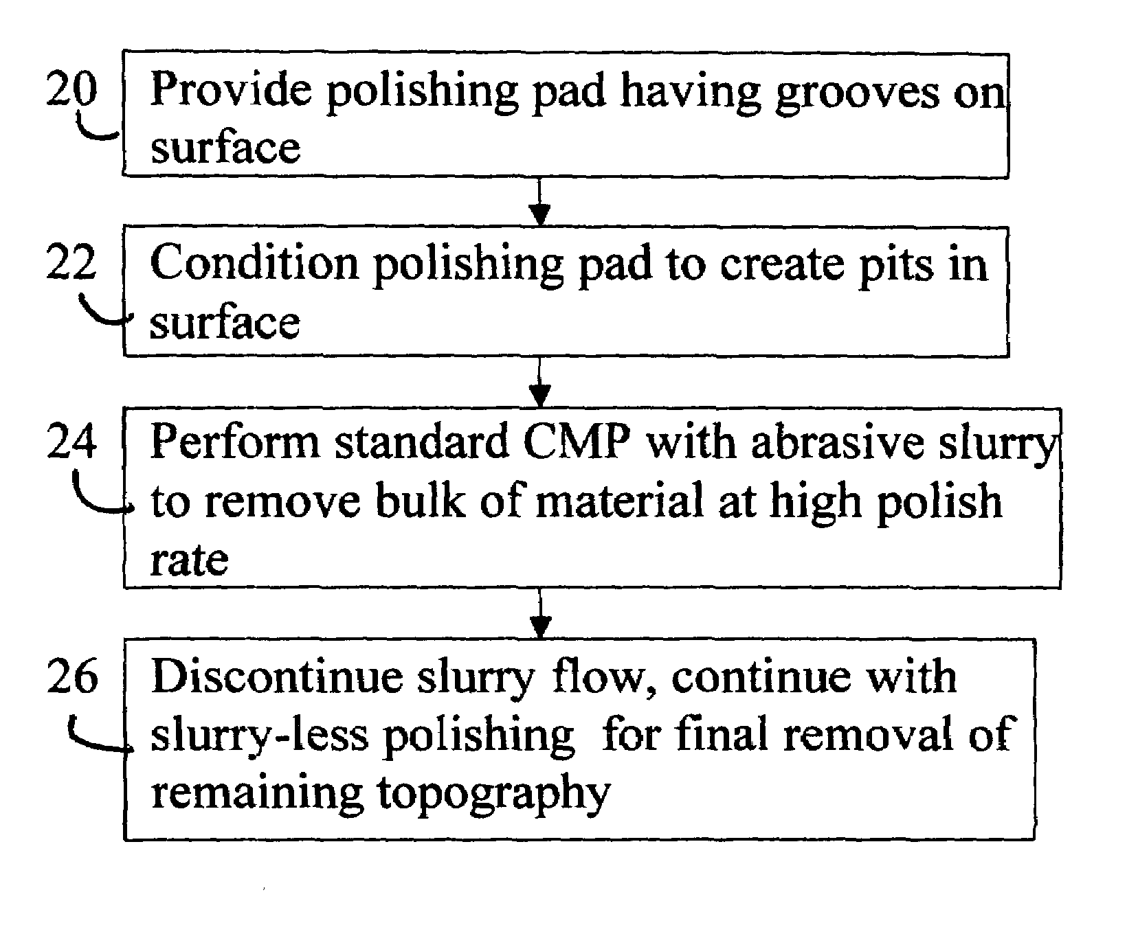
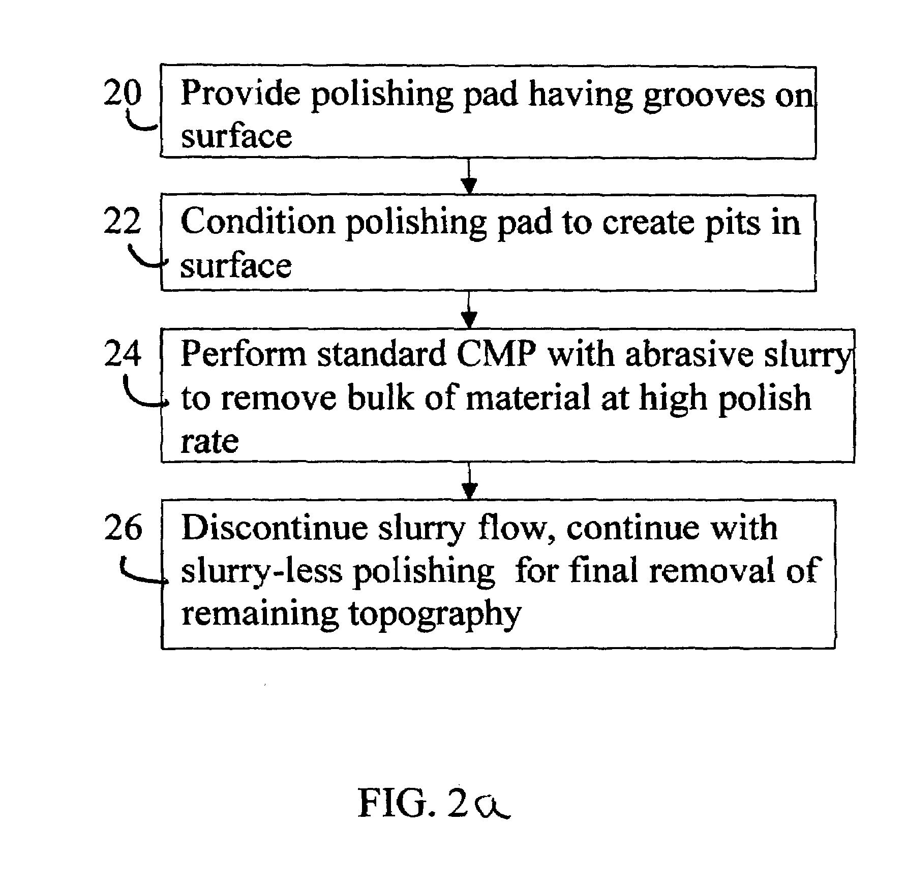
[0017]Our inventive process includes a two phase polish, the first of which utilizes a slurry, and the second of which is slurry-less. During the first phase utilizing slurry, fine abrasive particles are embedded into the polishing pad. During the second slurry-less phase, the fine embedded particles and the chemicals adsorbed / absorbed into the pad provide a very uniform final polish with much reduced dishing.

[0018]The process flow is shown in FIG. 2a and illustrated in FIG. 2b.

[0019]In step 20, a polyurethane polishing pad 200 having grooves on the polishing surface is provided. The IC1000 pad, commercially available from Rodel, Inc., having k-grooves, is a preferred alternative. Pads with other shaped grooves would also be acceptable. In fact, if step 22 is extended, pads without grooves will also be an alternative.

[0020]In step 22, the polishing pad is conditioned, by way of example by using a #20–200 grit diamond disc, to create and / or sustain a large number of pits or cavities...


PUM

PropertyMeasurementUnit
pressureaaaaaaaaaa
pressureaaaaaaaaaa
diameteraaaaaaaaaa

Abstract

A method for Chemical-Mechanical Polishing utilizes a two step process. The first step utilizes a slurry with abrasive particles which become embedded into a conditioned polishing pad having small cavities in the surface. During the second step the slurry flow is discontinued and the final polishing is performed using the embedded small abrasive particles. Using this method dishing has been reduced considerably, and has enabled the fabrication of a Damascene metal gate NMOSFET fabricated with Atomic Layer Deposition (ALD).

Description

FIELD OF THE INVENTION[0001]This invention relates to Chemical-Mechanical Polishing (CMP) and more particularly to the embedding of abrasive into polishing pads to reduce dishing and improve uniformity of polish.BACKGROUND OF THE INVENTION[0002]As integrated circuit devices shrink, and as circuit speed and performance increase, copper has replaced aluminum as the preferred electrical interconnect material. The use of copper as an interconnect material in silicon integrated circuits has occurred in response to the need for lowered interconnect resistivity, good electromigration resistance, and good deposition characteristics which allow effective filling of vias and contacts.[0003]Copper metallization structures are often formed by a process known as Damascene, wherein an interlevel dielectric layer (ILD) has regions etched therein into which metal lines will be inlaid. A barrier layer is deposited, which serves to prevent diffusion of copper from the metal lines into the dielectric....

Claims


Application Information

Patent Timeline
Patent Type & Authority Patents(United States)
IPC IPC(8): H01L21/302H01L21/461
CPCB24B37/042H01L21/3212H01L21/7684
Inventor XIE, JAMES J.SAHOTA, KASHMIR S.HUANG, RICHARD J.
Owner MOSAID TECH
Why Eureka
Try Eureka