Method of processing semiconductor wafer

a technology of semiconductor wafers and processing methods, applied in semiconductor/solid-state device testing/measurement, instruments, computing, etc., can solve problems such as inability to solve deviations in critical dimensions or other critical control variables within the wafer, inconsistent characteristics of the semiconductor wafers, etc., and achieve the effect of rectifying deviations

Active Publication Date: 2006-11-28
UNITED MICROELECTRONICS CORP
View PDF11 Cites 6 Cited by
  • Summary
  • Abstract
  • Description
  • Claims
  • Application Information

AI Technical Summary

Benefits of technology

[0007]According, at least one object of the present inventionis to provide a semiconductor wafer treatment method to effectively rectify a deviation within a same semiconductor wafer.
[0028]According to the semiconductor wafer treatment method of the present invention, performing a second manufacturing process subsequent to the first manufacturing process can compensate and remedy the deviation generated in the first manufacturing process.

Problems solved by technology

Further, each process step affects profoundly the critical dimension and the specification of the semiconductor device.
As a result, the characteristic of the semiconductor wafer is inconsistent.
Therefore, any the deviation in the critical dimensions or other critical control variables within a wafer can not be resolved.

Method used


Image

  • Method of processing semiconductor wafer
  • Method of processing semiconductor wafer
  • Method of processing semiconductor wafer

Examples


Embodiment Construction

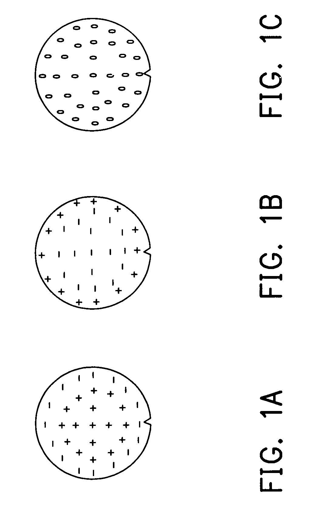
[0034]FIGS. 1A to 1C are are schematic diagrams of a wafer illustrating the distributions of critical dimensions across the wafer after a sequence of processes to demonstrate the basic concept of the present invention.

[0035]Referring to FIG. 1A, after a first manufacturing process is performed, the critical dimensions of the wafer are smaller than the average value at the peripheral region (as depicted by the symbol ‘−’), while the critical dimensions of wafer are greater than the average value at the center of the wafer (as depicted by the symbol ‘+’). After a first process deviation is determined, an adjustment is conducted in a second manufacturing process. As shown in FIG. 1B, the effect of the second manufacturing process on the same wafer includes providing the critical dimensions at the peripheral being greater than the average value (as depicted by the symbol ‘+’) and the critical dimensions at the center being smaller than the average value (as depicted by the symbol ‘−’). ...


PUM


Abstract

A method of processing a semiconductor wafer is provided. The semiconductor wafer is processed with a first process. After collecting the measured data that reflects the deviation of each part within the semiconductor wafer, the semiconductor wafer is processed with a second process according to the measured data to compensate the deviation from the first process and to correct any deviation in the semiconductor wafer.

Description

BACKGROUND OF THE INVENTION[0001]1. Field of the Invention[0002]The present invention relates to a semiconductor wafer treatment method. More particularly, the present invention relates to a treatment method for rectifying a deviation within a semiconductor wafer generated from a process.[0003]2. Description of Related Art[0004]With the current semiconductor manufacturing technology, multiple process steps are involved in the manufacturing of a semiconductor device, ranging from the manufacturing of semiconductor wafer materials to the packaging of the semiconductor device. Further, each process step affects profoundly the critical dimension and the specification of the semiconductor device. Therefore, the process parameters in each process step are carefully adjusted to effectively control the quality of the product.[0005]Advanced process control (APC) is an essential methodology used in maintaining and controlling critical processes during the fabrication of integrated circuits. I...

Claims


Application Information

Patent Timeline
Patent Type & Authority Patents(United States)
IPC IPC(8): G06F19/00
CPCH01L22/20
Inventor MA, HONGZHOU, MEISHENG
Owner UNITED MICROELECTRONICS CORP
Why Eureka
Try Eureka