Level shifter

a level shifter and shifter technology, applied in the direction of logic circuit coupling/interface arrangement, pulse technique, instruments, etc., can solve the problems of circuit characteristics degraded, pmos may not be fully turned off, corresponding circuit or device may erroneously operate, etc., to achieve fast rate, fast off operation, and fast rate

Active Publication Date: 2006-12-05
SK HYNIX INC
View PDF7 Cites 26 Cited by
  • Summary
  • Abstract
  • Description
  • Claims
  • Application Information

AI Technical Summary

Benefits of technology

[0018]Therefore, the present invention has been made in view of the above problems, and it is an object of the present invention to provide a level shifter that can reduce leakage current and avoid operation delay of a device by means of pull-up and pull-down drivers and that can implement a small-sized, lightweight and highly integrated device.
[0034]When an input signal level is shifted from a Vss level to a V1 level, a second N-channel Metal Oxide Semiconductor (NMOS) transistor at an output terminal of a pull-down driver is turned on and then a signal at a second node coupled to a drain of the second NMOS transistor is pulled down. At this point, a first P-channel Metal Oxide Semiconductor (PMOS) transistor at an input terminal of a pull-up driver receives the Vss level signal based on the pull-down operation from the second node through its gate and pulls up a signal at a first node coupled to the drain of the first PMOS transistor, such that a second PMOS transistor at the output terminal of the pull-up driver is turned off. Here, the present invention provides auxiliary pull-up means (or a predetermined switch device) between a source and a drain of the first PMOS transistor so that it can pull up a voltage of the first node at a fast rate. Thus, the second PMOS transistor can perform a fast OFF operation and a fast voltage level-shifting operation for the voltage at the second node and the output signal of the level shifter can be performed.
[0035]Moreover, when the input signal level is shifted from a V1 level to a Vss level, the first NMOS transistor at the input terminal of the pull-down driver is turned on and then a signal at the first node coupled to the drain of the first NMOS transistor is pulled down. At this point, the second PMOS transistor at the output terminal of the pull-up driver receives the Vss level signal based on the pull-down operation from the first node through its gate and pulls up a signal at the second node coupled to the drain of the second PMOS transistor, such that the first PMOS transistor at the input terminal of the pull-up driver is turned off. Here, the present invention provides auxiliary pull-up means (or a predetermined switch device) between the source and the drain of the second PMOS transistor so that it can pull up a voltage of the second node at a fast rate. Thus, the first PMOS transistor can perform a fast OFF operation and a fast voltage level-shifting operation for the voltage at the first node and the output signal of the level shifter can be performed.

Problems solved by technology

Otherwise, there is a problem in that a corresponding circuit or device may erroneously operate.
However, there is a problem in that the PMOS may not be fully turned off because of physical characteristics of the PMOS.
If the voltage at the source terminal of the PMOS is higher than that at the gate terminal of the PMOS and a voltage difference is less than the threshold voltage, there is another problem in that leakage current is incurred and hence circuit characteristics are degraded.
Thus, as an electric current channel is incurred between a V2 power supply and ground, there are problems in that leakage current is incurred and a voltage level-shifting operation for the output signal is delayed.
However, as the PMOS P2 and the NMOS N2 are simultaneously turned on because the PMOS P2 is not fully turned off and maintains the ON state for a predetermined time, an electric current channel is formed and hence leakage current may flow from the V2 power supply to the ground.
This leakage current causes operation delay when the voltage level at the node B is shifted from the V2 level to the Vss level.
Consequently, there is another problem in that the operation delay is incurred when the voltage level is shifted from the Vss level to the V2 level.
However, as the PMOS P1 and the NMOS N1 are simultaneously turned on because the PMOS P1 is not fully turned off and maintains the ON state for a predetermined time, an electric current channel is formed and hence leakage current may flow from the V2 power supply to the ground.
This leakage current causes operation delay when the voltage level at the node A is shifted from the V2 level to the Vss level.
Consequently, there is another problem in that the operation delay is incurred when the voltage level is shifted from the V2 level to the Vss level.
It can be seen that the above-described operation delay in the conventional level shifter is incurred.
However, because this method inherently increases device size to improve the electric current drive capabilities of the NMOS N1 and the NMOS N2, a layout area of the semiconductor device is increased and a highly integrated semiconductor device cannot be implemented.
When a voltage difference between the input and output signals is increased, there is a problem in that the size of the NMOS must be increased.
Moreover, there is another problem in that operation delay may be caused by an inappropriate operating state caused by an undesired electric current channel in the PMOS P1 and NMOS N1 or the PMOS P2 and NMOS N2.

Method used


Image

  • Level shifter
  • Level shifter
  • Level shifter

Examples


first embodiment

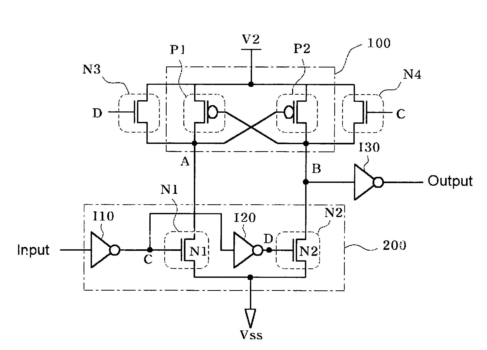
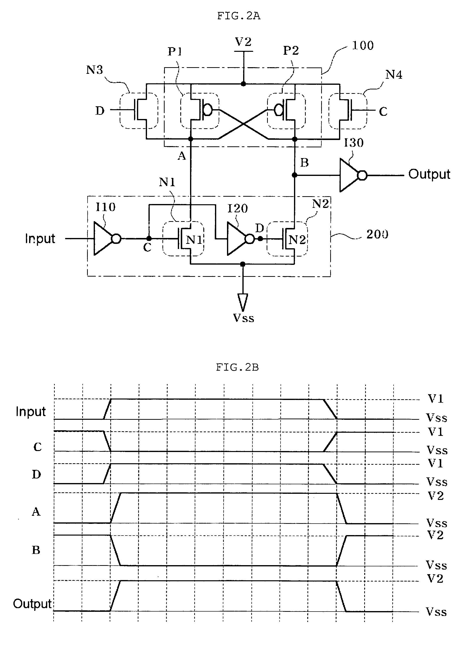
[0044]FIG. 2A is a circuit diagram illustrating a level shifter in accordance with the present invention.

[0045]As shown in FIG. 2A, the level shifter in accordance with the first embodiment of the present invention includes a pull-up driver 100 for pulling up a voltage level at a node A or B to a V2 level in response to an input signal; a pull-down driver 200 for pulling down the voltage level at the node A or B to a ground voltage level; and a plurality of auxiliary pull-up devices or switch devices coupled to the pull-up driver 100 for pulling up the voltage level at the node A or B. The level shifter further includes an inverter I10 for inverting the input signal; an inverter I20 for inverting a signal from the node C and outputting the inverted signal to a node D; and an inverter I30 for inverting a signal from the node B and outputting the inverted signal to an output terminal of the level shifter.

[0046]Here, the pull-up driver 100 includes a P-channel Metal Oxide Semiconductor...


PUM


Abstract

In a level shifter for receiving a signal of a first voltage level and outputting a signal of a second voltage level, a pull-down driver pulls down a voltage level at an output terminal of the level shifter to a ground voltage level. A pull-up driver and an auxiliary pull-up device pull up the voltage level at the output terminal to the second voltage level. The level shifter can reduce leakage current and avoid operation delay of a device through the pull-up and pull-down drivers and that can implement a small-sized, lightweight and highly integrated semiconductor memory device.

Description

BACKGROUND OF THE INVENTION[0001]1. Field of the Invention[0002]The present invention relates to a level shifter, and more particularly to a level shifter of a semiconductor memory device that can reduce leakage current and avoid operation delay of the device and that can implement a small-sized, lightweight and highly integrated device.[0003]2. Description of the Related Art[0004]A semiconductor memory device is a device capable of implementing Complementary Metal Oxide Semiconductor (CMOS) transistors and passive devices on a silicon wafer and writing and reading data. Most of the semiconductor devices are mounted on a board serving as an important element configuring a system. A semiconductor device externally receives an appropriate drive voltage (typically indicated by Vcc or Vdd). In some cases, a semiconductor device must internally generate a voltage less or higher than Vdd.[0005]In this case, circuits using power supply voltages with different voltage levels must be coupled...

Claims


Application Information

Patent Timeline
Patent Type & Authority Patents(United States)
IPC IPC(8): H03K19/0175G11C5/14H03K3/356
CPCH03K3/356113H03K3/356182Y02E60/14F28D20/00
Inventor KIM, SEUNG-LO
Owner SK HYNIX INC
Why Eureka
Try Eureka