Static magnetic field applying structure for use in atomic oscillator
a technology of atomic oscillator and applying structure, which is applied in the direction of oscillator, pulse automatic control, maser, etc., can solve the problems of affecting the operation of the static magnetic field generating circuit, the inability to design, and the inability to control the structure arrangement, etc., to achieve the effect of reducing the cost of production, facilitating the design of the structure, and facilitating the design
- Summary
- Abstract
- Description
- Claims
- Application Information
AI Technical Summary
Benefits of technology
Problems solved by technology
Method used
Image
Examples
first embodiment
[B] Description of First Embodiment
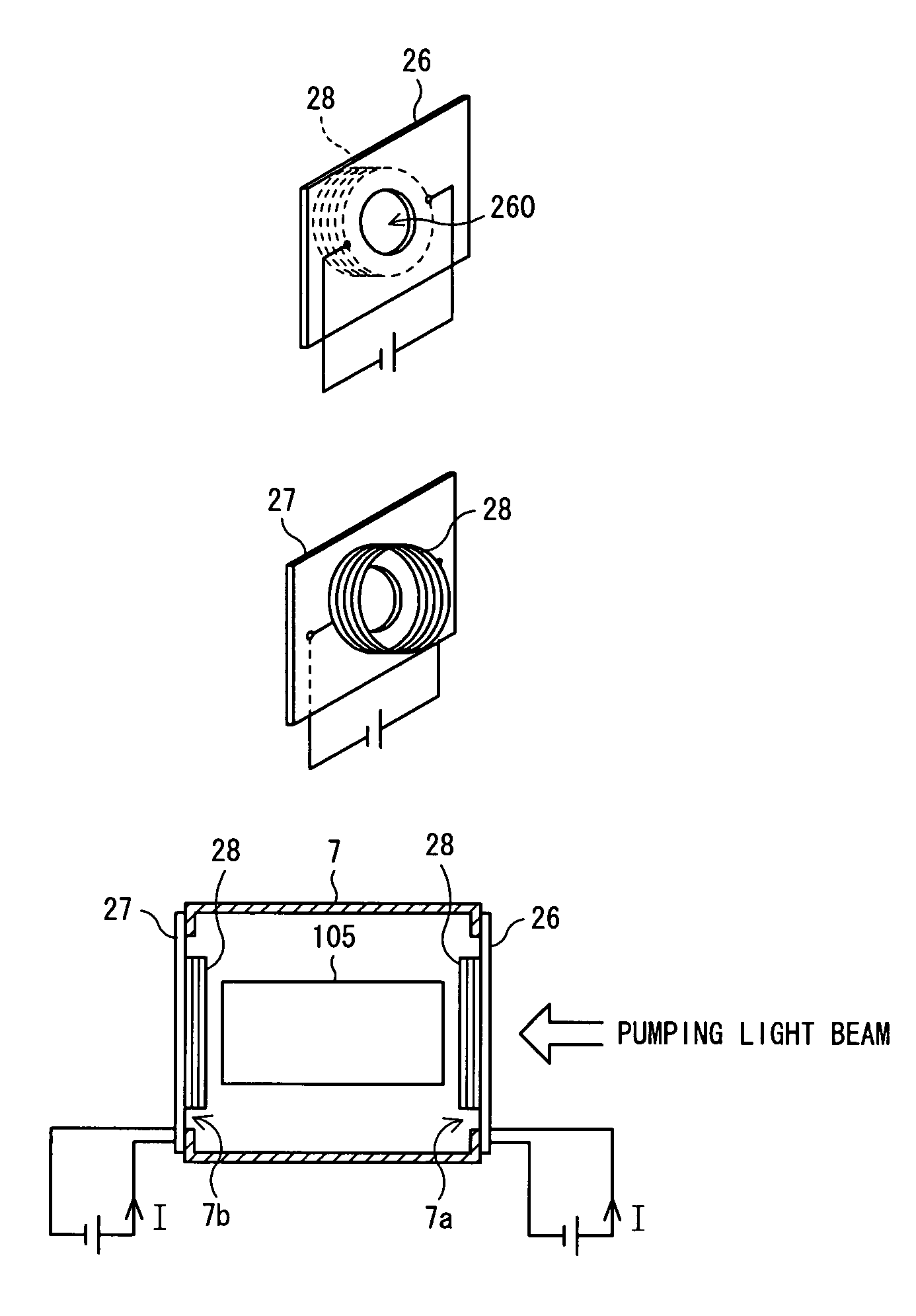
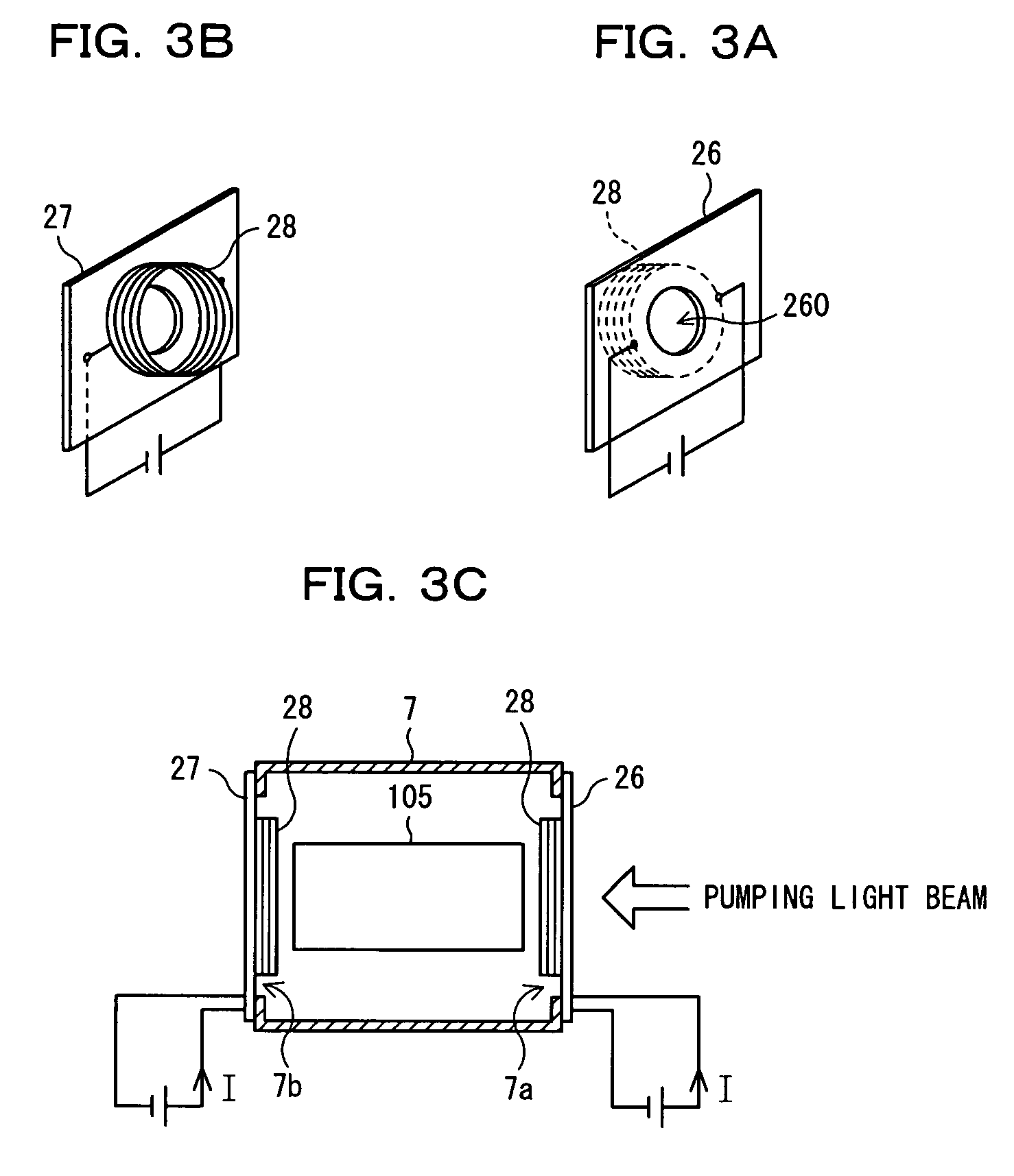
[0063]FIGS. 3A to 3C are diagrams showing a first embodiment of the present invention. As shown in FIGS. 3A to 3C, reference numerals 26 and 27 represent printed boards, 105 a resonance cell having atoms such as those of rubidium or cesium enclosed therein, 7 a cylindrical cavity resonator having the resonance cell 105 accommodated therein, respectively. The printed board (first printed board) 26 has provided an aperture (light beam passing aperture) 260 capable of leading a pumping light beam into the resonance cell 105 having the above atoms enclosed therein. As shown in FIG. 3B, the printed board (second printed board) 27 has an optical detector such as a PD (not shown) mounted thereon for monitoring the aforesaid pumping light beam. Further, both of the printed boards 26 and 27 have first and second coils (solenoid coils) 28 mounted thereon as magnetic field generating means, respectively, so that the first and second coils do not block the pas...
second embodiment
[C] Description of Second Embodiment
[0084]FIG. 8 is a set of diagrams each showing a second embodiment of the present invention. Of these diagrams, FIG. 8A is a schematic perspective view showing interlayer patterns 41, 42 and 43 of a multilayer (three layers) printed board 40. FIG. 8B is a schematic perspective view showing a construction realizing a static magnetic field generating circuit which is equivalent to one using the multilayer printed board 40 described with reference to FIG. 2. FIG. 8C is a schematic perspective view showing a construction provided with a resonance cell 105 in a static magnetic field created by the static magnetic field generating circuit shown in FIG. 8B.
[0085]As shown in FIG. 8A, an interlayer pattern 42 serving as an intermediate layer of the multilayer printed board 40 is composed of a straight conductive pattern (hereinafter referred to as straight pattern) 421 formed of a microstrip line (or strip line) and via holes 422 provided on both the sides...
PUM
 Abstract
Description
Claims
Application Information


