Micro-resonator based optical sensor

a micro-resonator and optical sensor technology, applied in the field of electro-electro-electro-electro-electro-electro-electro-electro-electro-electro-electro-electro-electro-electro-electro-electro-electro-electro-electro-electro-

Inactive Publication Date: 2006-12-05
LAMBDA CROSSING
View PDF14 Cites 54 Cited by
  • Summary
  • Abstract
  • Description
  • Claims
  • Application Information

AI Technical Summary

Problems solved by technology

These devices however suffer from a lack of sensitivity, which is often required in modern sensors.
Such a device requires a physical setup allowing for motion of the reflective surface with respect to the optical fiber, which may be difficult to accomplish.
Furthermore, the sensitivity of such a sensor is limited by the ratio of the reflective surface travel to the total cavity length.
Such a device may be difficult to manufacture, in that it typically requires two independent resonant polarization modes whose resonant frequencies must vary in different manners in response to parameter changes.
Furthermore, extraction of the parameter change requires complex characterization of the underlying sensor structure that is typically sensitive to process variations.
The further requirement for a narrow bandwidth, variable frequency light beam source, adds additional cost and complexity, as such a source is sensitive to environmental changes and thus requires stabilization or control.
The technique is somewhat limited to selective chemical interactions identifying the presence of target chemicals.

Method used


Image

  • Micro-resonator based optical sensor
  • Micro-resonator based optical sensor
  • Micro-resonator based optical sensor

Examples


first embodiment

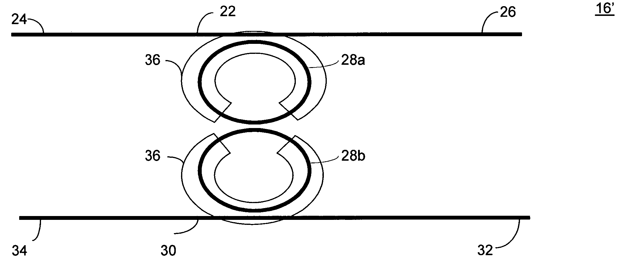
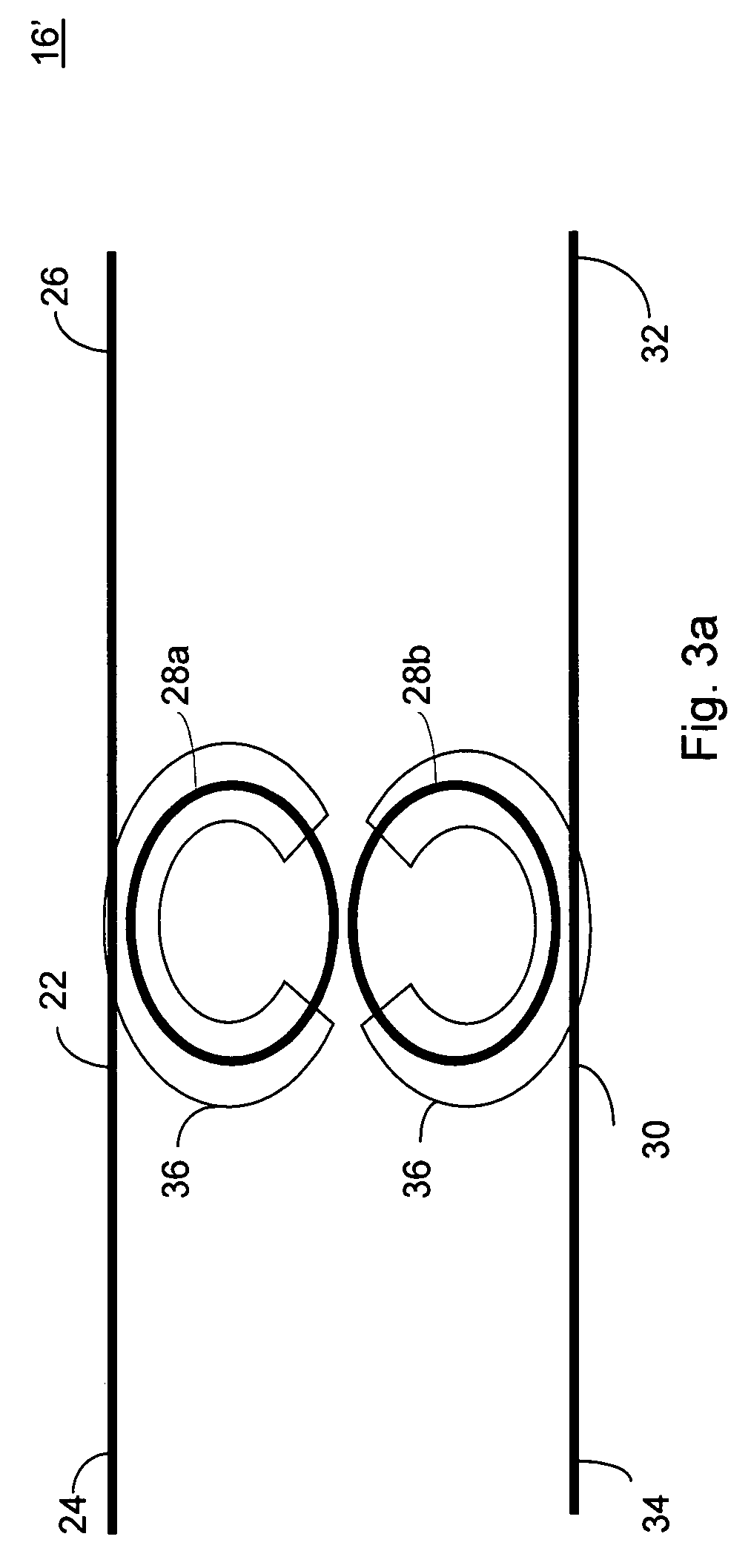
[0059]FIG. 3a illustrates a high level block diagram of an improved sensing element 16′ exhibiting enhanced sensitivity as compared with sensing element 16 of FIG. 2. Improved sensing element 16′ is operable to replace sensing element 16 of FIG. 1 and to be operable as part of sensing system 10. Sensing element 16′ comprises first optical waveguide 22 having input 24 and output 26, first sensing resonator cavity loop 28a, second sensing resonator cavity loop 28b, optional first and second tuning elements 36, and second optical waveguide 30 having input 34 and output 32. First optical waveguide 22 is placed in close proximity to at least a portion of first sensing resonator cavity loop 28a thus creating a first interaction area of evanescent coupling. At least a portion of second sensing resonator cavity loop 28b is placed in close proximity to at least a portion of first sensing resonator cavity loop 28a thus creating a second interaction area of evanescent coupling. Second waveguid...

second embodiment

[0065]FIG. 3b illustrates a high level block diagram of an improved sensing element 16′ exhibiting enhanced sensitivity. Improved sensing element 16′ is operable to replace sensing element 16 of FIG. 1 and to be operable as part of sensing system 10. Sensing element 16′ comprises input optical waveguide 14, reference resonator cavity loops 28e, 28f, optional first and second tuning elements 36, first optical waveguide 22 having output 26, first sensing resonator cavity loop 28a, second sensing resonator cavity loop 28b, optional third and fourth tuning elements 36, and second optical waveguide 30 having output 32. Input optical waveguide 14 is placed in close proximity to at least a portion of first reference resonator cavity loop 28e thus creating a first interaction area of evanescent coupling. First reference resonator cavity loop 28e is placed in close proximity to at least a portion of second reference resonator cavity loop 28f, thus creating a second interaction area of evanes...

third embodiment

[0069]FIG. 3c illustrates a high level block diagram of an improved sensing element 16′ exhibiting enhanced sensitivity. Improved sensing element 16′ is operable to replace sensing element 16 of FIG. 1 and to be operable as part of sensing system 10. Sensing element 16′ comprises input optical waveguide 14, reference resonator cavity loop 28e, first tuning element 36, first optical waveguide 22 having output 26, sensing resonator cavity loop 28a, optional second tuning element 36, and second optical waveguide 30 having output 32. Input optical waveguide 14 is placed in close proximity to at least a portion of reference resonator cavity loop 28e thus creating a first interaction area of evanescent coupling. First reference resonator cavity loop 28e is placed in close proximity to at least a portion of first optical waveguide 22 thus creating a second interaction area of evanescent coupling. First tuning element 36 is placed in proximity to reference resonator cavity loop 28e so as to...


PUM

PropertyMeasurementUnit
resonant frequencyaaaaaaaaaa
frequencyaaaaaaaaaa
areaaaaaaaaaaa

Abstract

An optical sensor system for providing an output signal in response to a sensed parameter is disclosed. The sensor system comprises an optical signal source generating an input signal, a sensing element in optical communication with the optical signal source and a detector in optical communication with the sensing element. The sensing element comprises at least two resonant cavity loops exhibiting a common resonant frequency near at least one frequency of the input signal, at least one of the resonant cavity loops being exposed to an external parameter. The external parameter modifies the resonant frequency of the at least one exposed resonant cavity loop thereby modifying an optical output signal. The detector detects any modification in the output optical signal in response to the sensed parameter.

Description

CROSS-REFERENCE TO RELATED APPLICATIONS[0001]This application claims priority from U.S. Provisional Patent Application Ser. No. 60 / 494,570 filed Aug. 13, 2003 entitled “Micro-Resonator Based Optical Sensor” whose entire contents are incorporated herein by reference.BACKGROUND OF THE INVENTION[0002]The invention relates generally to the field of electro-optical devices and in particular to an optical sensor which provides an output signal as a function of a change in a sensed physical parameter such as pressure, temperature, absorption or motion.[0003]Electro-optical devices have shown great promise in sensor applications. Passive optical sensors offer safe, accurate operation in hostile environments of heat and temperature, and are immune to electromagnetic interference. These advantages combine to make optically based sensors attractive for a number of applications.[0004]A wide variety of optical sensing techniques have been suggested for measuring physical parameters. These device...

Claims


Application Information

Patent Timeline
Patent Type & Authority Patents(United States)
IPC IPC(8): G01C19/72G01B9/02G01J1/04G01J1/42G01N21/45G01N21/77
CPCG01N21/45G01N21/7746
Inventor MARGALIT, MOTIBERKOWICZ, EYAL
Owner LAMBDA CROSSING
Why Eureka
Try Eureka