

Method for fabricating group-III nitride devices and devices fabricated using method
a technology of nitride and group-iii, which is applied in the direction of semiconductor/solid-state device manufacturing, semiconductor devices, electrical equipment, etc., can solve the problems of reducing the overall emitting efficiency of led, and difficulty in emitted light from led to the surroundings
- Summary
- Abstract
- Description
- Claims
- Application Information
AI Technical Summary
Benefits of technology
Problems solved by technology
Method used
Image

Examples
Embodiment Construction
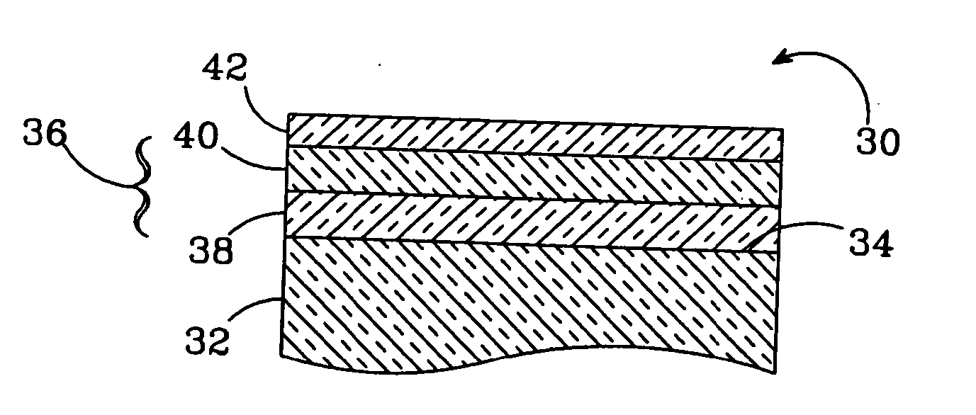
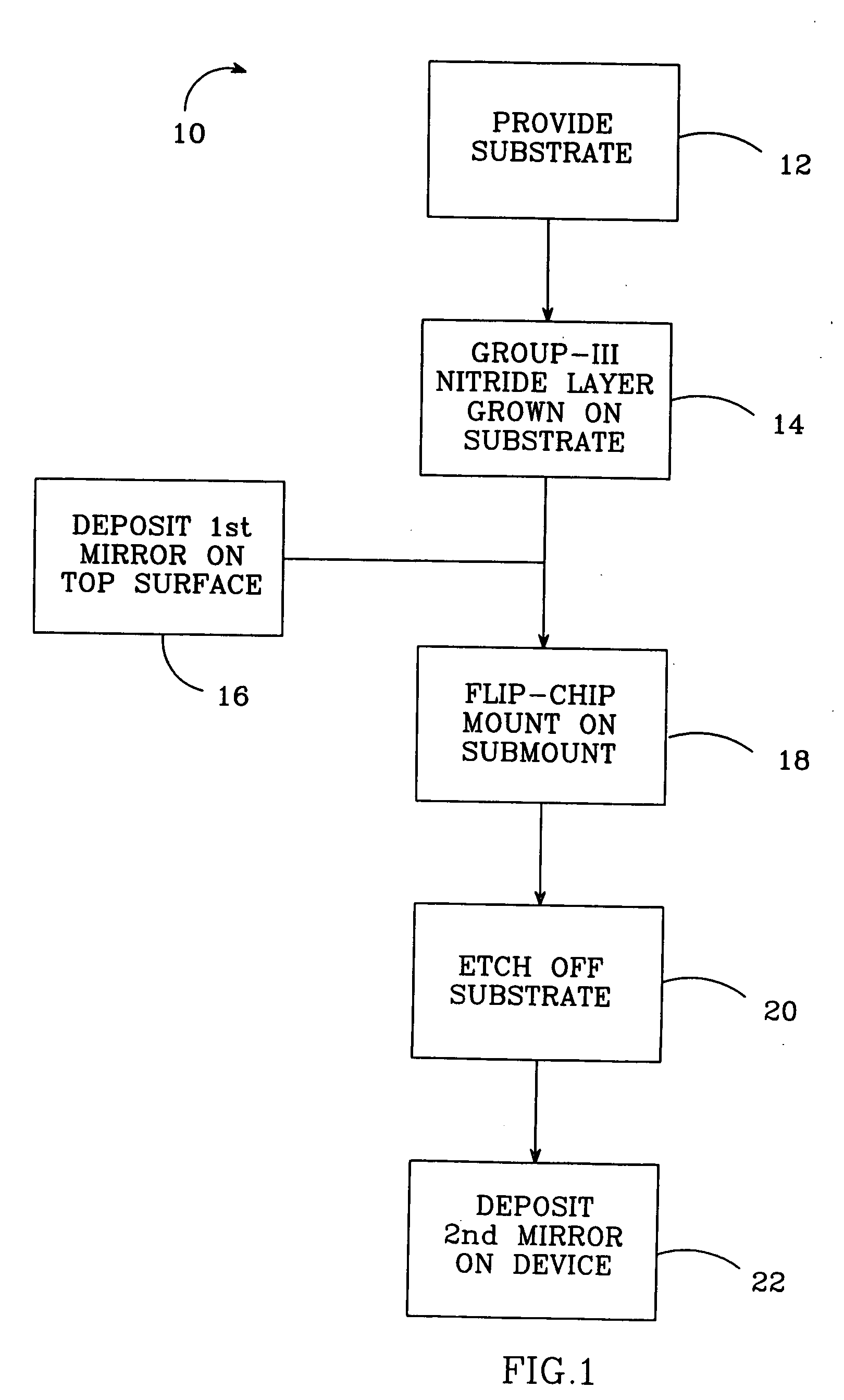
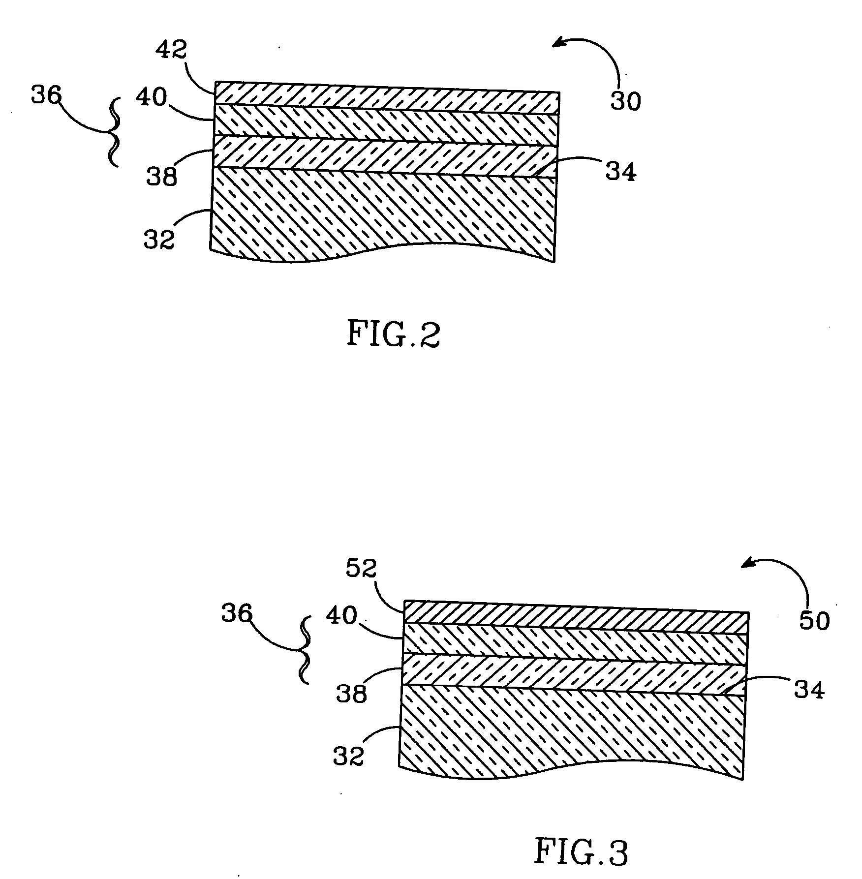
[0039]FIG. 1 shows one embodiment of a method 10 according to the present invention for fabricating Group-III nitride semiconductors, with the method 10 being particularly adapted for fabricating thin film Group-III nitride semiconductor devices. In step 12, a substrate is provided that can be made of many different materials, with a preferred material being silicon carbide. SiC is a suitable material for use with Group-III nitride materials, such as GaN, because it has a closer crystal lattice match to Group III nitrides GaN, which generally results in Group III nitride films of high quality. Silicon carbide also has high thermal conductivity so that the total output power of Group III nitride devices on silicon carbide is not limited by the thermal dissipation of the substrate (as is the case with some devices formed on sapphire). SiC substrates are available from Cree Research, Inc., of Durham, N.C. and methods for producing them are set forth in the scientific literature as well...
PUM
| Property | Measurement | Unit |
|---|---|---|
| electron velocity | aaaaa | aaaaa |
| angles | aaaaa | aaaaa |
| semiconductor | aaaaa | aaaaa |
Abstract
Description
Claims
Application Information