Metalized ceramic substrate, substrate manufacturing method and substrate and chip welding method

A technology of metallized ceramics and ceramic substrates, applied in semiconductor/solid-state device manufacturing, electrical components, electric solid-state devices, etc., can solve problems such as cracking of chips and metallization layers, failure of power electronic devices, chip shedding, etc., to achieve product Reduced size, high production accuracy, and reduced package thickness

Pending Publication Date: 2018-10-02
井敏
View PDF6 Cites 6 Cited by
  • Summary
  • Abstract
  • Description
  • Claims
  • Application Information

AI Technical Summary

Problems solved by technology

[0006] Aiming at the problems existing in the prior art that the metallized ceramic substrate will crack between the chip and the metallized layer under the impact of frequent changes in ambient temperature, causing the chip to fall off or break and cause power electronic devices to fail, this paper The invention provides a metallized ceramic substrate, a manufacturing method of the substrate and a welding method of the substrate and the chip, which can reduce the internal stress caused by the mismatch of thermal expansion coefficient between the metal and the chip as much as possible, and achieve the purpose of improving product reliability

Method used


Image

  • Metalized ceramic substrate, substrate manufacturing method and substrate and chip welding method
  • Metalized ceramic substrate, substrate manufacturing method and substrate and chip welding method
  • Metalized ceramic substrate, substrate manufacturing method and substrate and chip welding method

Examples


Embodiment 1

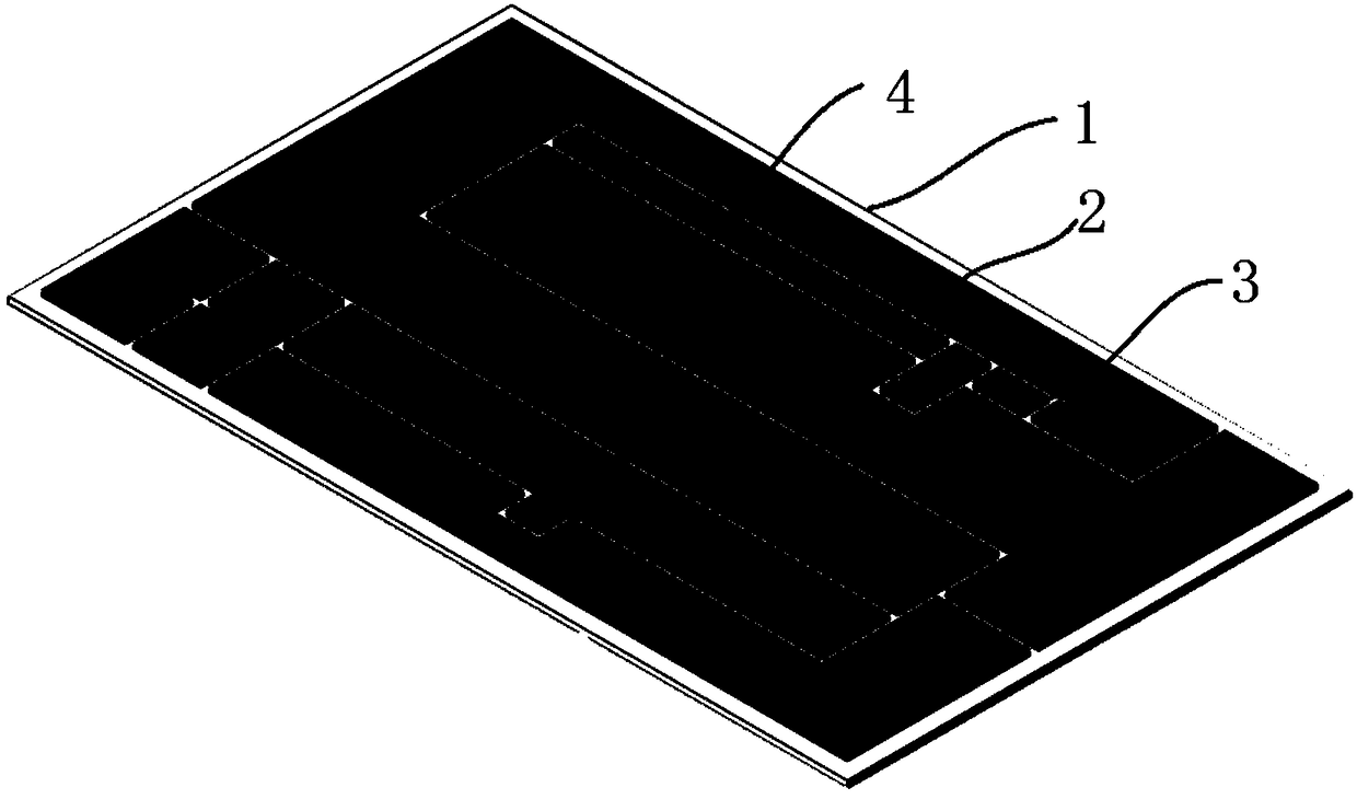
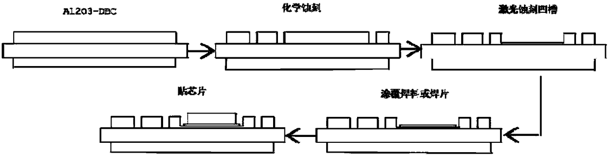
[0048] Such as figure 2 As shown, the Al with chip groove 4 2 O 3 --DBC metallized ceramic substrate and reliable welding method, this method includes the following steps:

[0049] S1, 138mm*190mm*0.38mm (copper sheet specification 134mm*184mm*0.30mm) specification Al 2 O 3 -DBC ceramic substrate, through the traditional chemical etching method to design the pattern on the Al 2 O 3 -The copper surface of DBC is processed.

[0050] S2. Position the chip accurately through the MARK point, and etch the chip groove of 15mm*15mm*0.28mm by laser etching.

[0051] S3. Coat Sn-Ag-Cu solder evenly on the copper surface at the bottom of the chip groove.

[0052] S4. Place the chip in the groove and heat it at 350°C for 20 minutes to complete the brazing. Since the chip groove 4 of the metalized ceramic substrate is small and easy to contact with adjacent circuits, the use of brazing can effectively ensure the accuracy of welding, prevent the solder from covering the circuit, and effectively en...

Embodiment 2

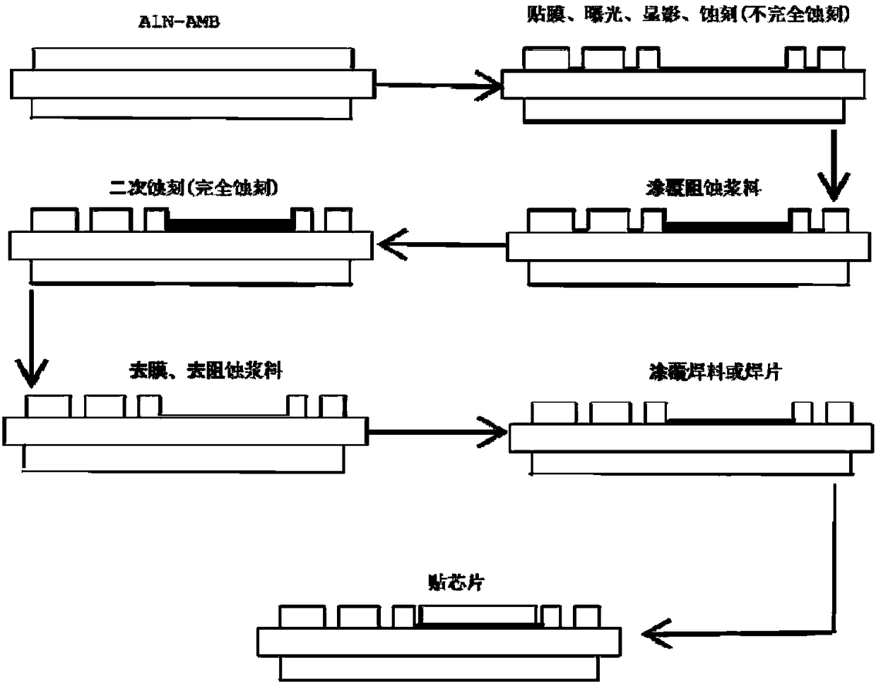
[0055] Such as image 3 As shown, the AlN-AMB metallized ceramic substrate with chip groove 4 and the reliability welding method, the method includes the following steps:

[0056] S1. The AlN-AMB substrate of 127mm*127mm*0.635mm (copper sheet specification 125mm*125mm*0.30mm) specifications is transferred to the copper layer through processes such as filming, exposure, and development.

[0057] S2. The pattern and groove are etched out by chemical etching, the etching depth is about 0.27mm, and the groove specification is 15mm*15mm.

[0058] S3. Cover the entire groove position with green oil, dry and harden.

[0059] S4. The remaining copper is quickly etched through the second chemical etching, the lines and grooves are processed, and then the film and the green oil are removed. At this time, the thickness of the groove metal layer is 0.03mm, which ensures the metal layer The coefficient of thermal expansion is small.

[0060] S5, and then evenly coat Sn-Ag-Cu solder on the copper su...

Embodiment 3

[0064] Such as Figure 4 As shown, the ZTA-DBA (Zirconium Oxide Toughened Alumina) metallized ceramic substrate with the chip groove 4 and the reliable welding method, this solution includes the following steps:

[0065] S1. Transfer the ZTA-DBA substrate of 138mm*190mm*0.32mm (aluminum sheet specification is 134mm*184mm*0.30mm) to the aluminum layer through filming, exposure, and development processes.

[0066] S2. The circuit is processed by chemical etching, and the etching depth is the thickness of the aluminum layer.

[0067] S3. Using mechanical processing, a groove of 15mm*15mm*0.28mm is processed at the chip position.

[0068] S4. Nickel is plated on the ZTA-DBA aluminum layer by electroless plating.

[0069] S5. Then evenly coat Sn-Ag-Cu solder on the bottom aluminum surface of the chip groove 4.

[0070] S6. Place the chip in the chip groove 4 and heat it at 350°C for 20 minutes to complete the brazing.


PUM

PropertyMeasurementUnit
thicknessaaaaaaaaaa
thicknessaaaaaaaaaa
etching depthaaaaaaaaaa

Abstract

The invention discloses a metalized ceramic substrate, a substrate manufacturing method and a substrate and chip welding method, belongs to the field of a semiconductor device, and specify to the problem of failure of a power electronic device caused by a cracking phenomenon between a chip and a metalized layer, and falling off or cracking of the chip due to frequent impact of cold and hot changesof environment temperature on the metalized ceramic substrate in the prior art. The invention provides the metalized ceramic substrate, the substrate manufacturing method and the substrate and chip welding method; the metalized ceramic substrate comprises a ceramic substrate; a metal layer is arranged on one or two surfaces of the ceramic substrate; a circuit is arranged on the metal layer; a chip groove is formed in a metal layer chip mounting position; and the chip is welded on the chip groove of the manufactured metalized ceramic substrate through a brazing technique. By virtue of the method, internal stress caused by mismatch of thermal expansion coefficients between the metal layer and the chip can be lowered as far as possible, and product reliability is improved.

Description

Technical field [0001] The invention relates to the field of semiconductor components, and more specifically, to a metalized ceramic substrate, a method for manufacturing the substrate, and a method for welding the substrate and a chip. Background technique [0002] The metalized ceramic substrate is a new type of substrate in the semiconductor field. The current common packaging form is to directly solder the chip on the surface of the metalized layer. However, this kind of substrate has many technical defects: because the metallization thickness is greater than or equal to 100μm, under the impact of frequent cold and hot changes in the ambient temperature, cracks will occur between the chip and the metallization layer, causing the chip to fall off or break Power electronic devices fail. The main reason for this situation is that the thermal expansion coefficient of the metal layer does not match the silicon chip. [0003] The Chinese patent application, application number 20152...

Claims


Application Information

Patent Timeline
Patent Type & Authority Applications(China)
IPC IPC(8): H01L23/498H01L21/48H01L21/60
CPCH01L23/49838H01L24/83H01L21/4846H01L2224/832H01L2224/83192
Inventor 井敏
Owner 井敏
Why Eureka
Try Eureka