Method of etching surface layer portion of silicon wafer and method of analyzing metal contamination of silicon wafer

Active Publication Date: 2012-03-29
SUMCO CORP
View PDF6 Cites 5 Cited by
  • Summary
  • Abstract
  • Description
  • Claims
  • Application Information

AI Technical Summary

Benefits of technology

[0012]An aspect of the present invention provides for means for rapidly and uniformly

Problems solved by technology

As semiconductor devices have become smaller and more highly integrated in the field of semiconductor manufacturing, trace metal impurities on the surface of the semiconductor substrate have been reported to affect device characteristics by producing leak defects and gate oxide integrity defects, shortening service lifetime, and the like.
Further, not just contamination by metal impurities on the surface of the semiconductor substrate, but trace metal impurity contamination in areas of the surface layer of a semiconductor wafer on which device structures such as shallow trenches, sources, and drains are formed are also viewed as problems that affect device characteristics.
However, when employing the liquid phase etching method, uniform etching of the surface layer of a silicon wafer requires a large quantity of acid solution.
Accordingly, inadequate sensitivity results from dilution of the metal impurity concentration by the large quantity of acid solution employed.
Further, decreased sensitivity results from a heightened analysis background because of the introduction of contaminants from the acid solution itself.
Both of these hinder highly sensitive analysis in the field of semiconductor manufacturing field, in which the evaluati

Method used


Image

  • Method of etching surface layer portion of silicon wafer and method of analyzing metal contamination of silicon wafer
  • Method of etching surface layer portion of silicon wafer and method of analyzing metal contamination of silicon wafer
  • Method of etching surface layer portion of silicon wafer and method of analyzing metal contamination of silicon wafer

Examples


Example

Example 1

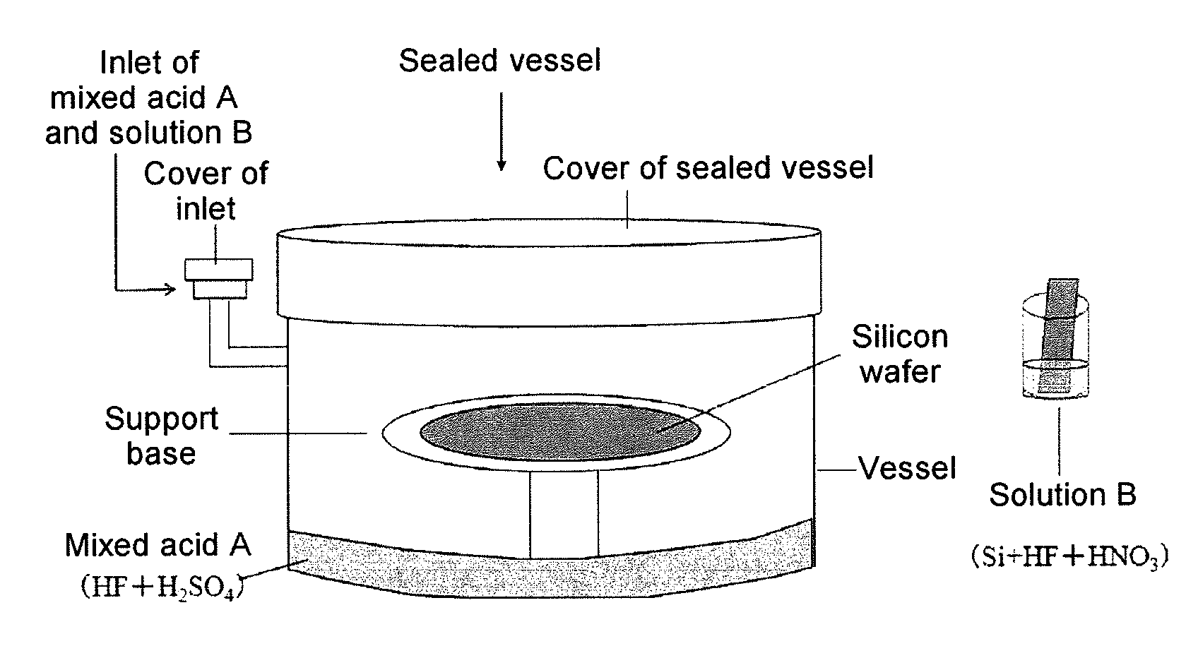
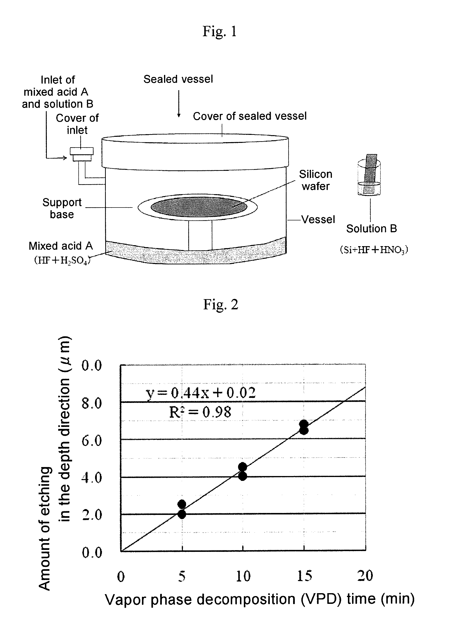
[0063]To the vessel shown in FIG. 1 (30 cm in diameter×15 cm in height, made of polyvinyl chloride) was charged a mixed acid comprising 500 g of hydrofluoric acid (EL grade 50 percent) and 200 g of sulfuric acid (EL grade 98 percent). A silicon wafer 200 mm in diameter with top and bottom surfaces that had been processed to mirror finishes was then positioned on a support base made of PTFE, and the cover was installed to seal the vessel. The vessel was left standing for five minutes to allow the mixed acid to generate HF.

[0064]Separately from the above operation, a 0.3 g piece of silicon (L×W×H: 10 cm×5 cm×0.07 cm) was dissolved by immersion for two minutes in a mixed acid comprising 90 g of nitric acid (EL grade 68 percent) and 10 g of hydrofluoric acid (EL grade 50 percent) in a 250 mL beaker (8 cm in diameter).

[0065]Next, the solution in the beaker was introduced into the sealed vessel through a tube via an inlet provided in the lateral surface of the vessel. Subsequentl...

Example

Comparative Example 1

[0068]A mixed acid comprising 400 g of sulfuric acid (EL grade 98 percent), 180 g of nitric acid (EL grade 68 percent), and 1,000 g of hydrofluoric acid (EL grade 50 percent) containing a 1 g piece of silicon was placed in a sealed square vessel (L×W×H=45 cm×30 cm×15 cm) and silicon wafers identical to those in Example 1 were subjected to VPD for 15 minutes. FIG. 4 shows a schematic of the etching process in Comparative Example 1.

[0069]Subsequently, the thickness in a linear direction running through the center of the wafers was measured in the same manner as in Example 1. The results are given in FIG. 5. As will be understood from FIG. 5, with a difference in the in-plane thickness of about 8 μm, the results indicated poor in-plane etching uniformity in the direction of depth.

[0070]A comparison of FIGS. 3 and 5 reveals that in Example 1, etching was conducted with a more uniform amount of wafer in-plane etching than in Comparative Example 1. FIG. 6 shows a digi...

Example

Example 2

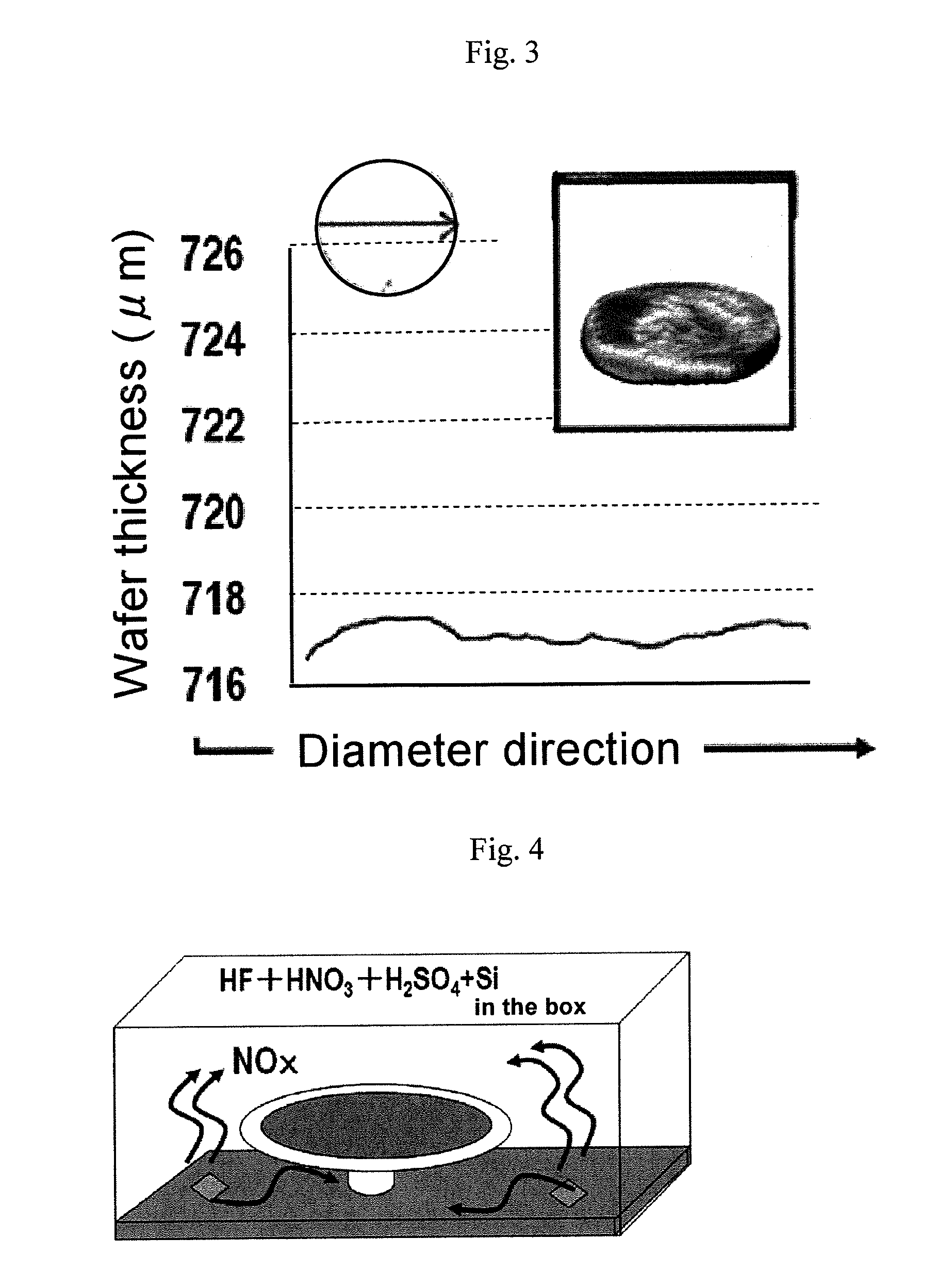
[0071]A silicon wafer 200 mm in diameter with surfaces processed to mirror finishes that had been contaminated by spin coating with a quantity of Mo of about 1E+13 atoms / cm2 was annealed for 90 minutes at 950° C. in a nitrogen atmosphere and then cleaned with hydrofluoric acid. Subsequently, it was subjected to five cycles of vapor phase etching by the same method as in Example 1. With the completion of each cycle of vapor phase etching, the cover was removed from the sealed vessel, the silicon wafer was removed, 100 μl of an acidic collection liquid comprising 5 percent hydrofluoric acid / 10 percent hydrochloric acid / 5 percent hydrogen peroxide solution was applied dropwise to the surface of the etched wafer, the liquid was scanned over the entire surface of the wafer, and the metal impurities were collected. The collected solution was mixed with 1,000 μl of ultrapure water, and quantitative evaluation of Mo was conducted by high-sensitivity double-focusing ICP-MS.

[0072]FIG...


PUM


Abstract

An aspect of the present invention relates to a method of etching a surface layer portion of a silicon wafer comprising: positioning the silicon wafer within a sealed vessel containing a mixed acid A of hydrofluoric acid and sulfuric acid so that the silicon wafer is not in contact with mixed acid A; introducing a solution B in the form of nitric acid containing nitrogen oxides into the sealed vessel and causing solution B to mix with mixed acid A; and vapor phase decomposing the surface layer portion of the silicon wafer within the sealed vessel within which mixed acid A and solution B have been mixed.

Description

CROSS-REFERENCE TO RELATED APPLICATIONS[0001]This application claims the benefit of priority under 35 USC 119 to Japanese Patent Application No. 2010-215058, filed on Sep. 27, 2010, which is expressly incorporated herein by reference in its entirety.BACKGROUND OF THE INVENTION[0002]1. Field of the Invention[0003]The present invention relates to a method of etching a surface layer portion of a silicon wafer, more particularly, to a method of etching a surface layer portion of a silicon wafer that is suitable as a method of etching a surface layer portion of a silicon wafer to analyze metal contamination of the silicon wafer. Still more particularly, the present invention relates to an etching method that is capable of etching a surface layer portion of a silicon wafer in the direction of depth thereof with in-plane uniformity.[0004]The present invention further relates to a method of analyzing metal contamination of a silicon wafer employing the above etching method.[0005]2. Discussi...

Claims


Application Information

Patent Timeline
IPC IPC(8): H01L21/66H01L21/306
CPCG01N1/32H01L22/12H01L21/30604
Inventor WU, JIAHONGMOHAMMAD, SHABANI B.
Owner SUMCO CORP
Why Eureka
Try Eureka