Semiconductor laser devices and methods

a laser device and semiconductor technology, applied in semiconductor lasers, laser details, semiconductor devices, etc., can solve the problems of fundamental limitations of bipolar transistor speed, spontaneous emission recombination lifetime, etc., to promote carrier transport unidirectionally, improve the directionality and speed of carrier transport, light emission and device speed are both enhanced

Inactive Publication Date: 2007-10-23
THE BOARD OF TRUSTEES OF THE UNIV OF ILLINOIS
View PDF16 Cites 66 Cited by
  • Summary
  • Abstract
  • Description
  • Claims
  • Application Information

AI Technical Summary

Benefits of technology

[0008]Another aspect of the prior copending applications involves employing stimulated emission to advantage in the base layer of a bipolar transistor (e.g. a bipolar junction transistor (BJT) or a heterojunction bipolar transistor (HBT), in order to enhance the speed of the transistor. Spontaneous emission recombination lifetime is a fundamental limitation of bipolar transistor speed. In an embodiment of the prior copending applications, the base layer of a bipolar transistor is adapted to enhance stimulated emission (or stimulated recombination) to the detriment of spontaneous emission, thereby reducing recombination lifetime and increasing transistor speed. In a form of this embodiment, at least one layer exhibiting quantum size effects, preferably a quantum well or a layer of quantum dots, preferably undoped or lightly doped, is provided in the base layer of a bipolar transistor. At least a portion of the base layer containing the at least one layer exhibiting quantum size effects, is highly doped, and of a wider bandgap material than the at least one layer. The at least one quantum well, or layer of quantum dots, within the higher gap highly doped material, enhances stimulated recombination and reduces radiative recombination lifetime. A two-dimensional electron gas (“2-DEG”) enhances carrier concentration in the quantum well or quantum dot layer, thereby improving mobility in the base region. Improvement in base resistance permits reduction in base thickness, with attendant reduction of base transport time. As described in the prior copending applications, these advantages in speed are applicable in high speed bipolar transistors in which light emission is utilized, and / or in high speed bipolar transistors in which light emission is not utilized. In light emitting bipolar transistor devices, for example heterojunction bipolar transistors of direct bandgap materials, the use of one or more layers exhibiting quantum size effects can also be advantageous in enhancing light emission and customizing the emission wavelength characteristics of the devices.
[0010]In another embodiment disclosed in the prior copending applications, a plurality of spaced apart quantum size regions (e.g. quantum wells and / or quantum dots) having different thicknesses are provided in the base region of a bipolar transistor and are used to advantageously promote carrier transport unidirectionally through the base region. As an example, the base region can be provided with several spaced apart quantum size regions of different thicknesses, with the thicknesses of the quantum size regions being graded from thickest near the collector to thinnest near the emitter. An injected electron is captured in a smaller well, tunnels into the next bigger well, and then the next bigger well, and so forth, until, at the biggest well closest to the collector, it tunnels to and relaxes to the lowest state of the biggest well and recombines. The arrangement of wells encourages carrier transport unidirectionally from emitter toward collector. Maximum recombination and light are derived from the biggest well as near as possible to the collector, which is an advantageous position, such as for optical cavity reasons. Carriers diffuse “downhill” in energy; i.e., toward the thicker wells. The asymmetry in well size provides improved directionality and speed of carrier transport. In a light emitting HBT, light emission and device speed are both enhanced.

Problems solved by technology

Spontaneous emission recombination lifetime is a fundamental limitation of bipolar transistor speed.

Method used


Image

  • Semiconductor laser devices and methods
  • Semiconductor laser devices and methods
  • Semiconductor laser devices and methods

Examples


Embodiment Construction

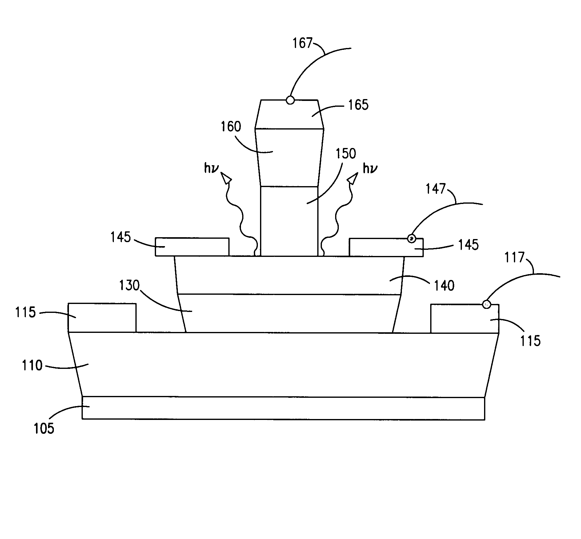
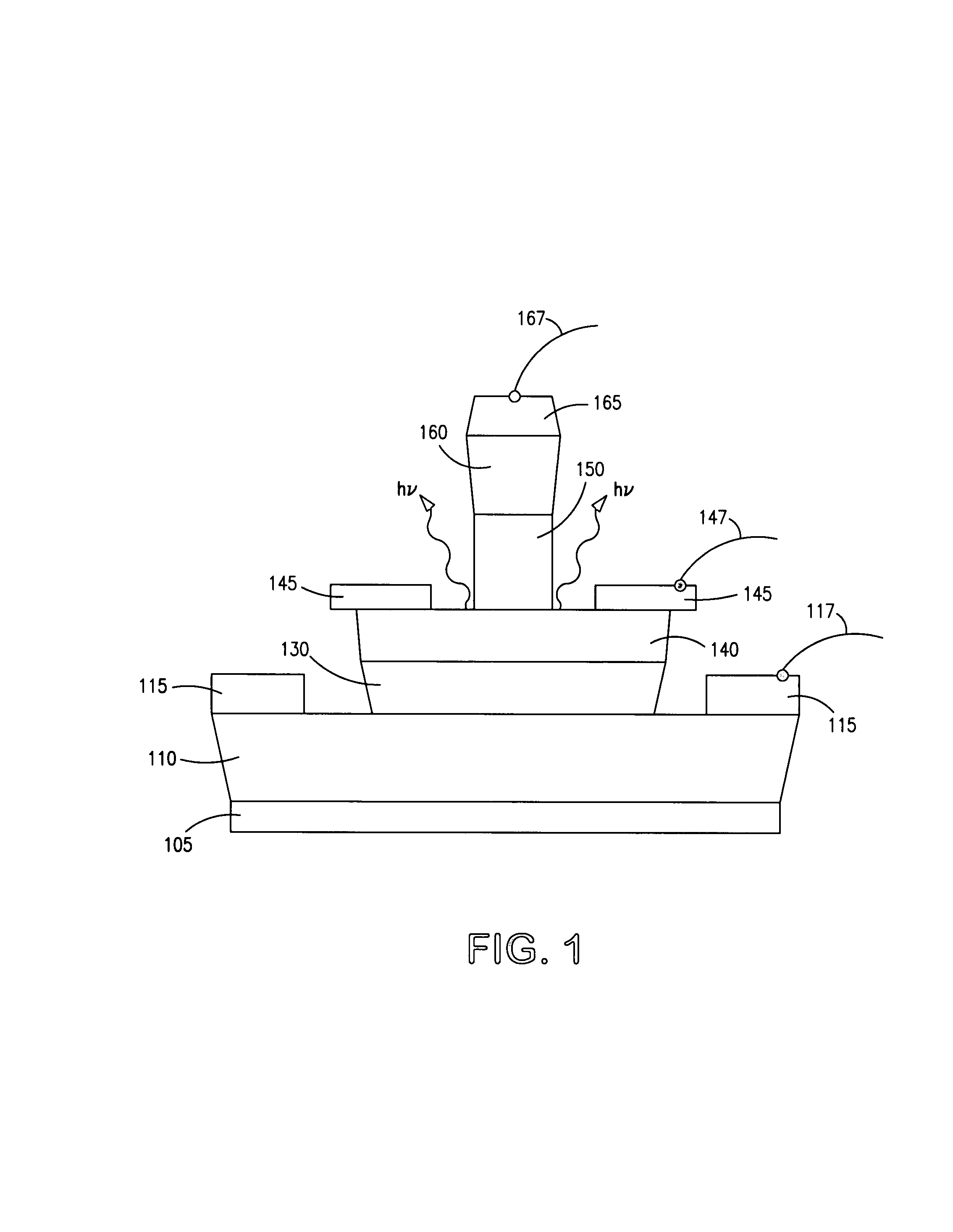
[0033]FIG. 1 illustrates a device as set forth in the above-referenced copending application Ser. No. 10 / 646,457. A substrate 105 has the following layers disposed thereon: subcollector 110, collector 130, base 140, emitter 150, and cap layer 160. Also shown are collector metallization (or electrode) 115, base metallization 145, and emitter metallization 165. Collector lead 117, base lead 147, and emitter lead 167 are also shown. As described in the referenced copending application, the collector layer 130 comprises 3000 Angstrom thick n-type GaAs, n=2×1016 cm−3, the base layer 140 comprises 600 Angstrom thick p+ carbon-doped compositionally graded InGaAs (1.4% In), p=4.5×1019 cm−3, the emitter layer 150 comprises 800 Angstrom thick n-type InGaP, n=5×1017 cm−3, and the cap layer comprises 1000 Angstrom thick n+ InGaAs, n=3×1019 cm−3.

[0034]As described in the referenced copending application, for conventional PN junction diode operation, the recombination process is based on both an ...


PUM


Abstract

A method for producing controllable light pulses includes the following steps: providing a heterojunction bipolar transistor structure including collector, base, and emitter regions of semiconductor materials; providing an optical resonant cavity enclosing at least a portion of the transistor structure; and coupling electrical signals with respect to the collector, base, and emitter regions, to switch back and forth between a stimulated emission mode that produces output laser pulses and a spontaneous emission mode. In a form of the method, the electrical signals include an AC excitation signal, and part of each excitation signal cycle is operative to produce stimulated emission, and another part of each excitation signal cycle is operative to produce spontaneous emission.

Description

PRIORITY CLAIMS[0001]The present application is a continuation-in-part of U.S. patent application Ser. No. 10 / 861,103, filed Jun. 4, 2004 now U.S. Pat. No. 7,091,082 (which is, in turn, a continuation-in-part of U.S. patent application Ser. No. 10 / 646,457, filed Aug. 22, 2003, now abandoned), and the present application is also a continuation-in-part of U.S. patent application Ser. No. 10 / 861,320, filed Jun. 4, 2004 (which is, in turn, a continuation-in-part of U.S. patent application Ser. No. 10 / 646,457, filed Aug. 22, 2003, now abandoned).GOVERNMENT RIGHTS[0002]This invention was made with Government support under Contract Number HR0011-04-1-0034 awarded by the Defense Advanced Research Projects Agency (DARPA). The Government has certain rights in the invention.FIELD OF THE INVENTION[0003]This invention relates to semiconductor laser devices and methods, and also to a laser transistor and techniques for enhancing high speed optical signal generation.BACKGROUND OF THE INVENTION[000...

Claims


Application Information

Patent Timeline
Patent Type & Authority Patents(United States)
IPC IPC(8): H01S3/13
CPCB82Y20/00H01L33/0016H01S5/06203H01L33/08H01S5/0422H01S5/0618H01S5/34313H01S5/06226H01S5/06812H01S5/305H01S5/3054H01S5/3211
Inventor FENG, MILTONHOLONYAK, JR., NICKCHAN, RICHARDWALTER, GABRIEL
Owner THE BOARD OF TRUSTEES OF THE UNIV OF ILLINOIS
Why Eureka
Try Eureka