Pad surface finish for high routing density substrate of BGA packages

Inactive Publication Date: 2006-12-12
ALTERA CORP
View PDF2 Cites 21 Cited by
  • Summary
  • Abstract
  • Description
  • Claims
  • Application Information

AI Technical Summary

Benefits of technology

[0007]The present invention is directed to a new bonding pad structure for reducing the likelihood of cracks in the Cu/Sn intermetallic layer. In a preferred embodiment of the invention, the bonding pad structure includes a copper pad and a pad surface finish comprising multiple layers of solder. The multiple layers of solder include at least a layer of eutectic solder (or a layer of pure-Sn solder) covering the copper pad and a thicker layer of high-Pb solder covering the layer of eutectic s

Problems solved by technology

Since the layer of high-Pb solder is thicker than the eutectic solder layer (or the layer of pure-

Method used


Image

  • Pad surface finish for high routing density substrate of BGA packages
  • Pad surface finish for high routing density substrate of BGA packages
  • Pad surface finish for high routing density substrate of BGA packages

Examples


Embodiment Construction

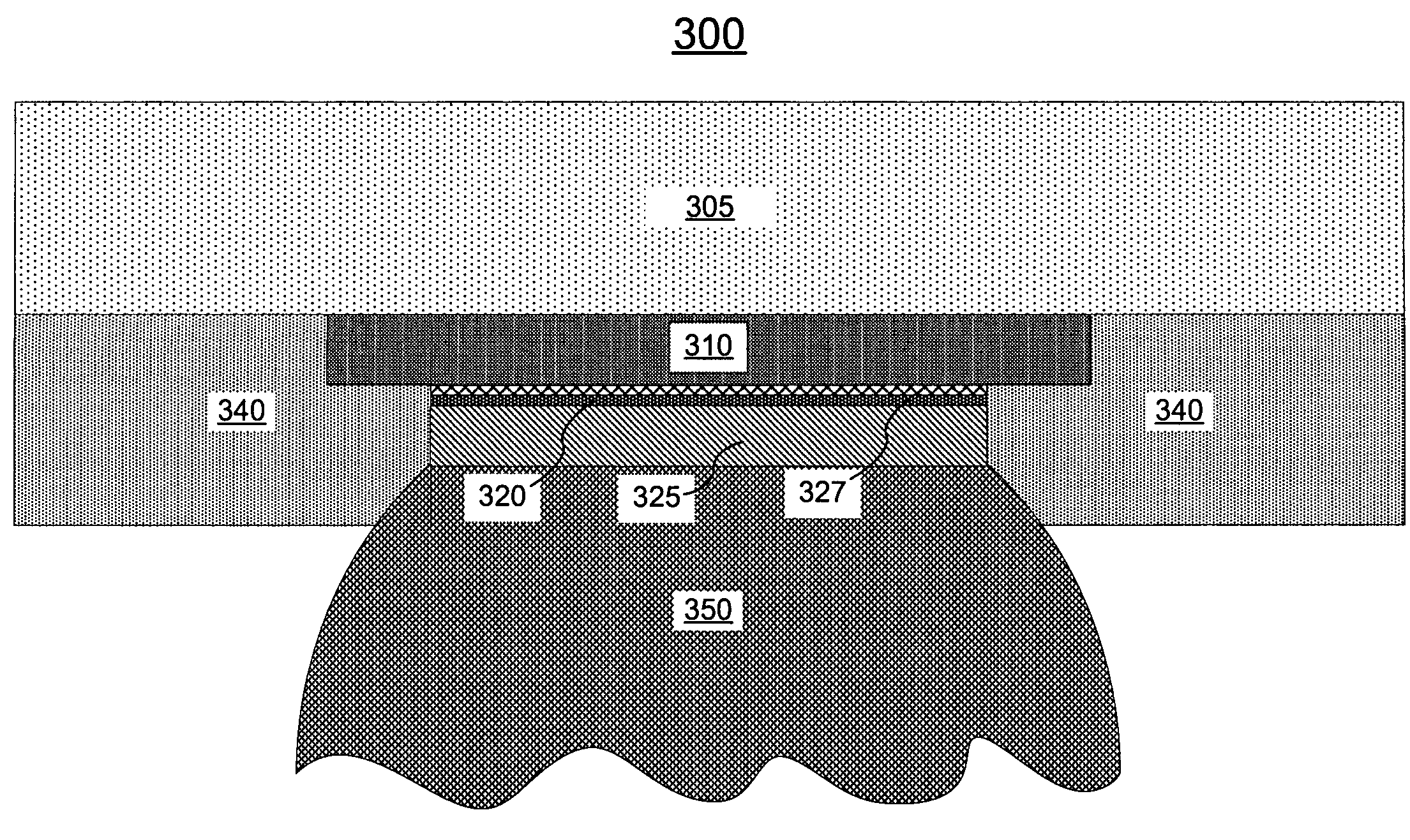
[0014]FIG. 3A is an enlarged cross-sectional view of a bonding pad structure 300 formed according to one embodiment of the present invention. While bonding pad structure 300 is shown formed on the bottom side of a substrate 305, it can also be formed on the top side of substrate 305. Compared with the SOP finish 230 in FIG. 2A, this bonding pad structure has a different type of pad surface finish that includes multiple layers of solder. This structure is formed by first depositing a layer of eutectic solder 320 on the surface of the copper pad 310 through processes such as screen printing or plating. This layer covers the copper pad. Second, a layer of high-Pb solder 325 is deposited on the surface of the layer of eutectic solder 320 again using processes such as screen printing or plating. The composition of the high-Pb solder is at least 80% lead and at most 20% tin. In one embodiment, the composition of the high-Pb solder is 95% lead and 5% tin. The layer of high-Pb solder 325 is...


PUM


Abstract

The present invention is directed to a new bonding pad structure that includes a copper pad and a pad surface finish comprising multiple layers of solder. The multiple layers of solder include at least a layer of eutectic solder (or a layer of pure-Sn solder) covering the copper pad and a layer of high-Pb solder covering the layer of eutectic solder (or the layer of pure-Sn solder). Since the layer of high-Pb solder is significantly thicker than the eutectic solder layer (or the layer of pure-Sn solder), there is insufficient tin supply in the eutectic solder (or the layer of pure-Sn solder) for forming a thick Cu/Sn intermetallic layer on the copper pad. Instead, a thin Cu/Sn intermetallic layer is formed on the copper pad and there is less likelihood of forming a crack in the thin Cu/Sn intermetallic layer.

Description

[0001]The present invention relates generally to an electronic package and, in particular, to a new bonding pad surface finish that can be used to create a ball grid array (BGA) substrate having a high routing density.BACKGROUND OF THE INVENTION[0002]This relates to electronic packages that contain an integrated circuit (IC) typically fabricated on a semiconductor die. The package protects the IC from the environment and provides I / O interfaces for the IC to communicate with other circuits.[0003]FIG. 1 is a cross-sectional view of a prior art BGA package including a BGA substrate 100 and a semiconductor die 120 on the surface of the substrate 100. The semiconductor die carries an electronic circuit, e.g., a programmable logic device (PLD). The substrate includes a multitude of conductive paths running from an array of solder bumps 130 on one side of the substrate to an array of solder balls 160 on the other side of the substrate. The array of solder bumps 130 is located between the ...

Claims


Application Information

Patent Timeline
IPC IPC(8): H01L23/48H01L23/52
CPCH01L23/49816H01L23/498H01L2924/0002H01L2924/00
Inventor WANG, WEN-CHOU VINCENT
Owner ALTERA CORP
Why Eureka
Try Eureka