Method of making a semiconductor device that has copper damascene interconnects with enhanced electromigration reliability

a technology of damascene and semiconductor devices, applied in semiconductor devices, semiconductor/solid-state device details, electrical equipment, etc., can solve problems such as open-circuit failure, copper layer, and impractical solution to electromigration problems

Inactive Publication Date: 2006-12-26
INTEL CORP
View PDF7 Cites 18 Cited by
  • Summary
  • Abstract
  • Description
  • Claims
  • Application Information

AI Technical Summary

Problems solved by technology

Such electromigration can cause vacancies, which may lead to voids.
If a void grows to a size that creates metal separation, e.g., near a via that contacts the conductor, it may cause an open-circuit failure.
That solution to the electromigration problem is impractical, however, because ...

Method used


Image

  • Method of making a semiconductor device that has copper damascene interconnects with enhanced electromigration reliability
  • Method of making a semiconductor device that has copper damascene interconnects with enhanced electromigration reliability
  • Method of making a semiconductor device that has copper damascene interconnects with enhanced electromigration reliability

Examples


Embodiment Construction

[0006]A method for making a semiconductor device is described. That method comprises forming a copper containing layer on a substrate, then forming an alloying layer that includes an alloying element on the copper containing layer. After applying heat to cause an intermetallic layer that includes copper and the alloying element to form on the surface of the copper containing layer, a barrier layer is formed on the intermetallic layer. In the following description, a number of details are set forth to provide a thorough understanding of the present invention. It will be apparent to those skilled in the art, however, that the invention may be practiced in many ways other than those expressly described here. The invention is thus not limited by the specific details disclosed below.

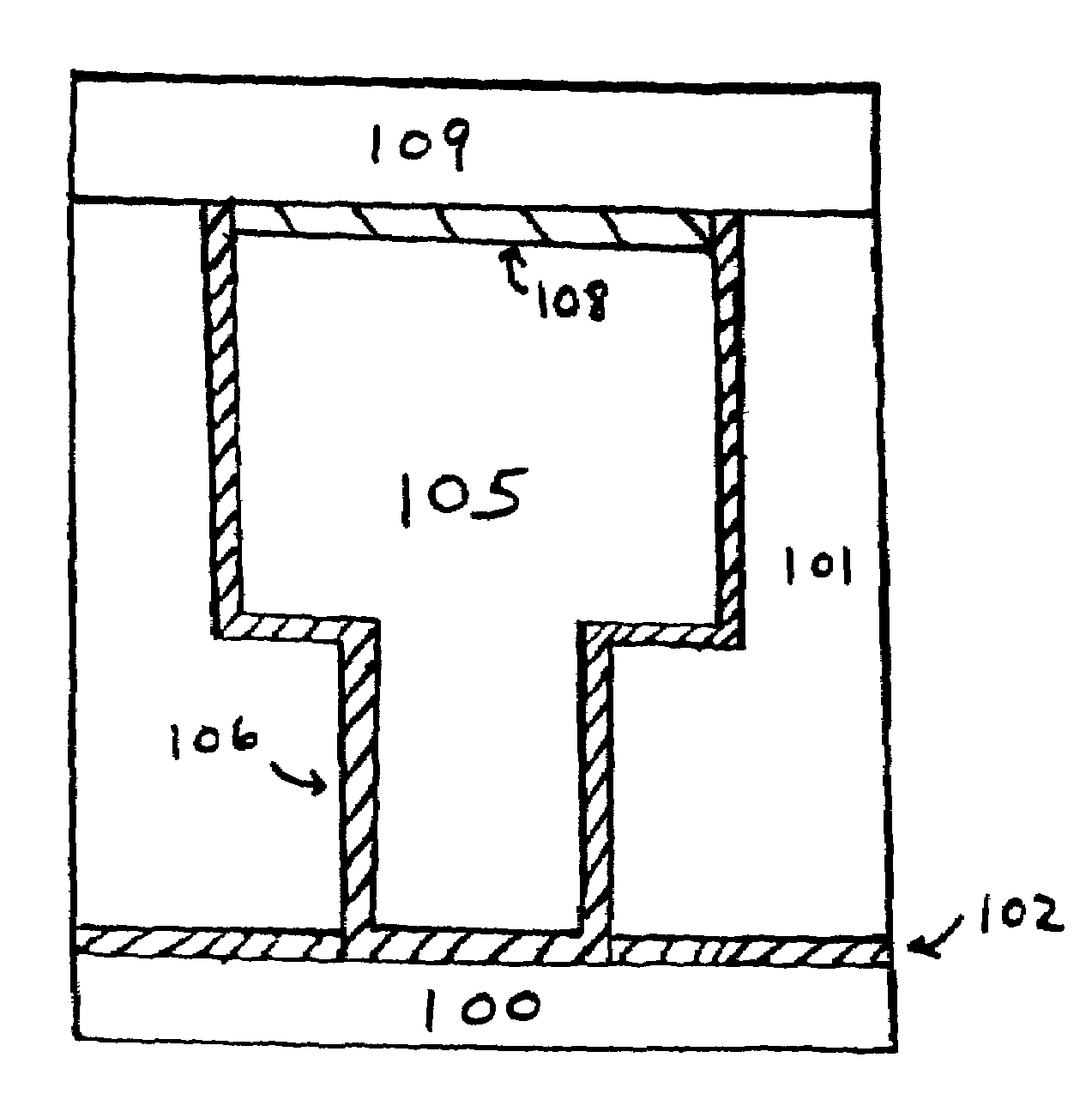
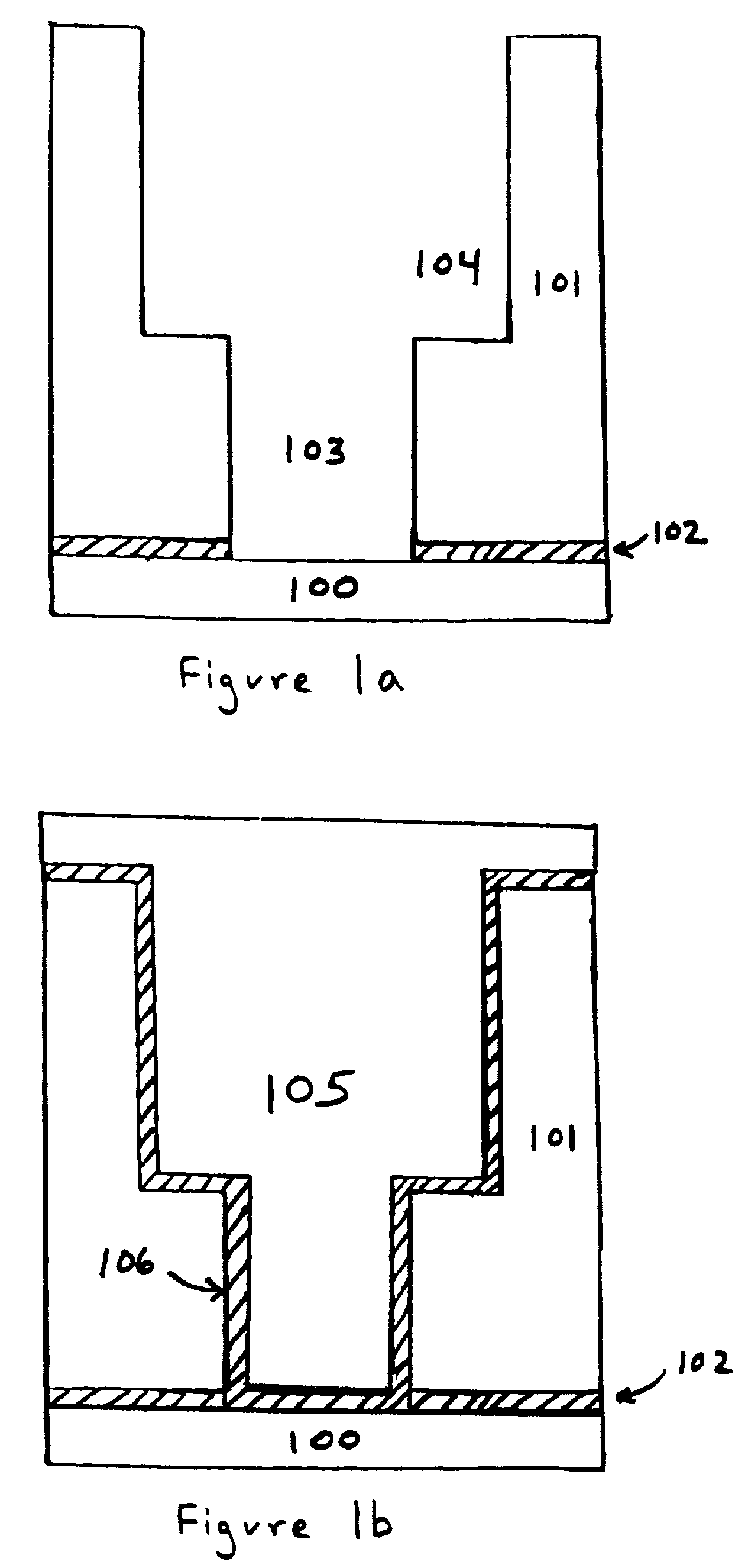
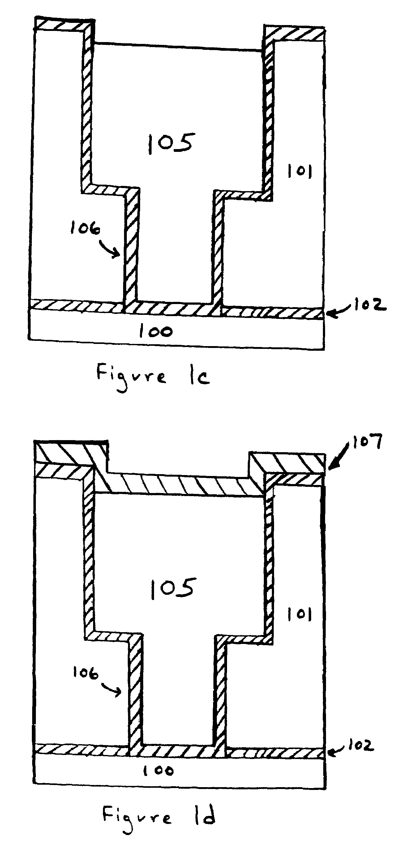
[0007]FIGS. 1a–1f represent cross-sections of structures that may be formed when making a semiconductor device using the method of the present invention to reduce electromigration in a copper conductor. FIG. ...


PUM


Abstract

A method of making a semiconductor device is described. That method includes forming a copper containing layer on a substrate, and forming an alloying layer that includes an alloying element on the copper containing layer. After applying heat to cause an intermetallic layer that includes copper and the alloying element to form on the surface of the copper containing layer, a barrier layer is formed on the intermetallic layer.

Description

FIELD OF THE INVENTION[0001]The present invention relates to a method of making semiconductor devices, in particular, devices that include copper damascene interconnects.BACKGROUND OF THE INVENTION[0002]When making advanced semiconductor devices, copper interconnects may offer a number of advantages over those made from aluminum. For that reason, copper has become the material of choice for making such devices' interconnects. As device dimensions shrink so does conductor width—leading to higher resistance and current density. Increasing current density can increase the rate at which copper atoms are displaced when current passes through a copper conductor. Such electromigration can cause vacancies, which may lead to voids. Those voids may form at the interface between the copper conductor and a barrier layer that is formed on the conductor. If a void grows to a size that creates metal separation, e.g., near a via that contacts the conductor, it may cause an open-circuit failure.[000...

Claims


Application Information

Patent Timeline
IPC IPC(8): H01L21/44H01L21/768
CPCH01L21/76849H01L21/76858
Inventor HAU-RIEGE, STEFANHAU-RIEGE, CHRISTINEZHENG, WEN-YUE
Owner INTEL CORP
Why Eureka
Try Eureka