Method for making a semiconductor device having a high-k gate dielectric layer and a metal gate electrode

a metal gate electrode and dielectric layer technology, applied in the direction of semiconductor devices, electrical equipment, transistors, etc., can solve the problems that the gate dielectric of the very thin gate dielectric made of silicon dioxide may experience unacceptable gate leakage currents and adversely affect the physical and electrical properties of the transistor

Active Publication Date: 2006-12-26
INTEL CORP
View PDF42 Cites 87 Cited by
  • Summary
  • Abstract
  • Description
  • Claims
  • Application Information

AI Technical Summary

Problems solved by technology

MOS field-effect transistors with very thin gate dielectrics made from silicon dioxide may experience unacceptable gate leakage currents.
Because, however, such a dielectric may not be compatible with polysilicon, it may be desirable to use metal gate electrodes in devices that include high-k gate dielectrics.
Because this process requires multiple etch, deposition, and polish steps, high volume manufacturers of semiconductor devices may be reluctant to use it.
Unfortunately, the exposed sidewalls of the resulting high-k gate dielectric layer render that layer susceptible to lateral oxidation, which may adversely affect its physical and electrical properties.

Method used


Image

  • Method for making a semiconductor device having a high-k gate dielectric layer and a metal gate electrode
  • Method for making a semiconductor device having a high-k gate dielectric layer and a metal gate electrode
  • Method for making a semiconductor device having a high-k gate dielectric layer and a metal gate electrode

Examples


Embodiment Construction

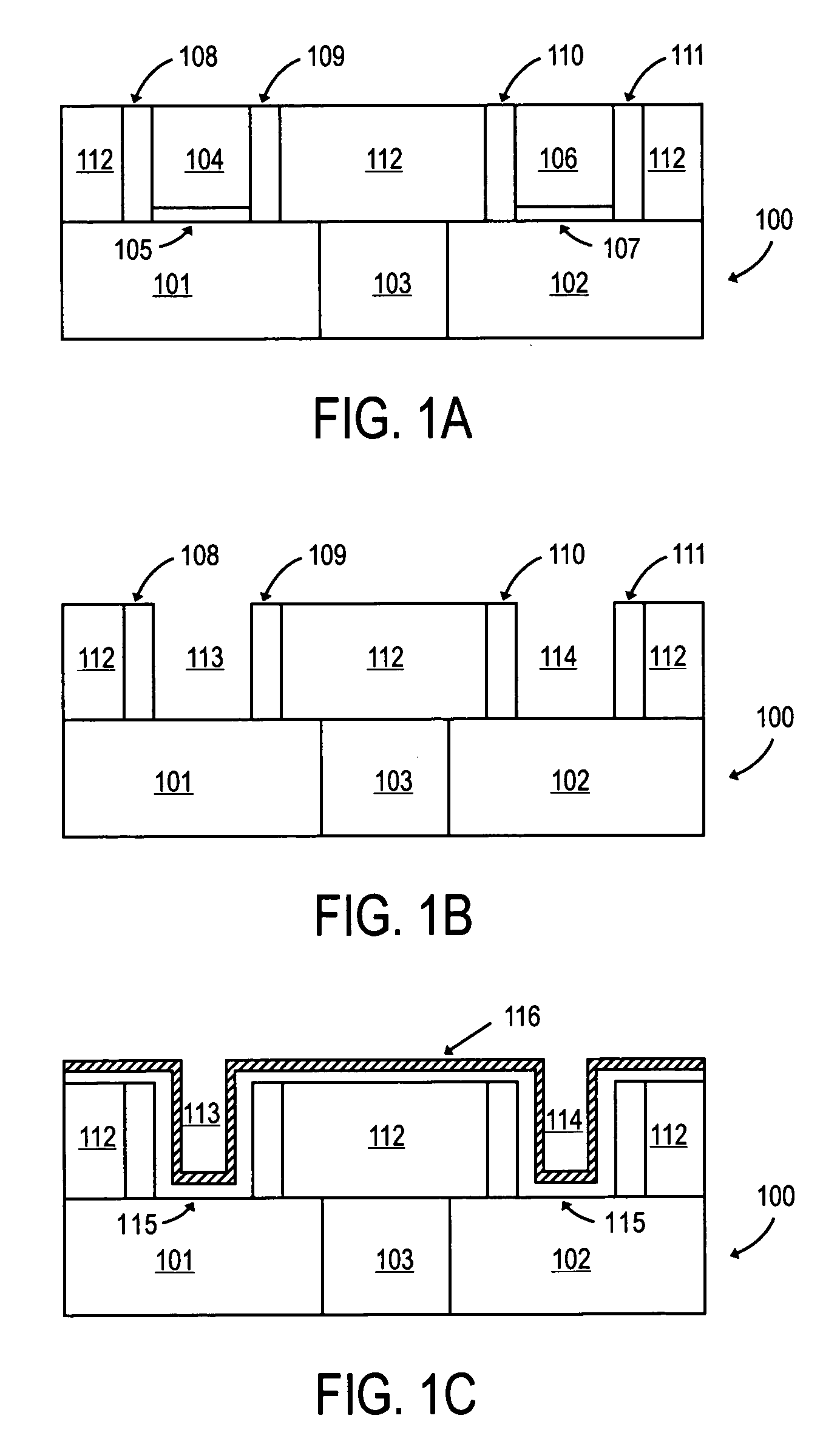
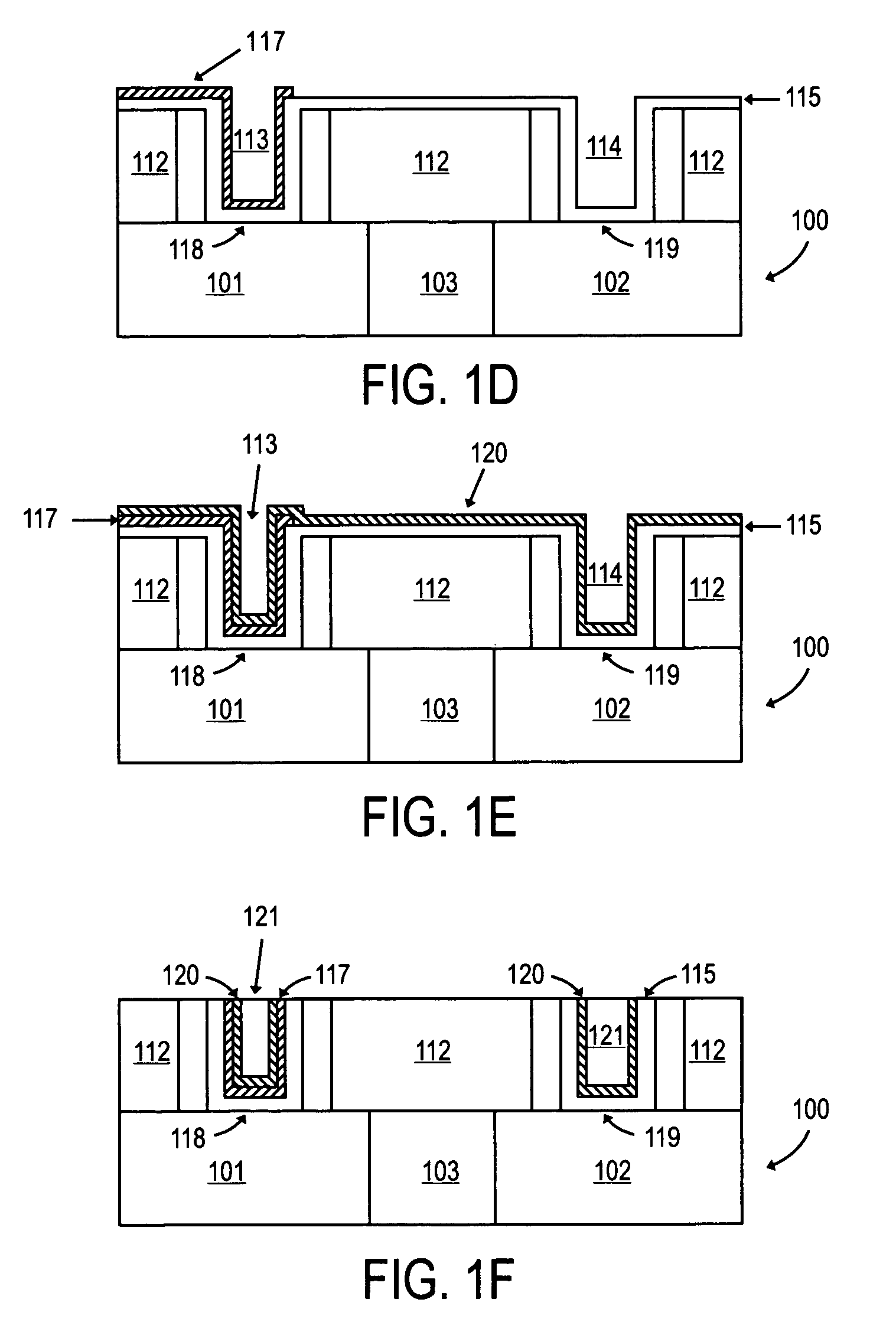
[0011]A method for making a semiconductor device is described. That method comprises forming a first dielectric layer on a substrate, then forming a trench within the first dielectric layer. After forming a second dielectric layer on the substrate, a first metal layer is formed on a first part of the second dielectric layer, but not on a second part of the second dielectric layer. A second metal layer is then formed on the first metal layer and on the second part of the second dielectric layer.

[0012]In the following description, a number of details are set forth to provide a thorough understanding of the present invention. It will be apparent to those skilled in the art, however, that the invention may be practiced in many ways other than those expressly described here. The invention is thus not limited by the specific details disclosed below.

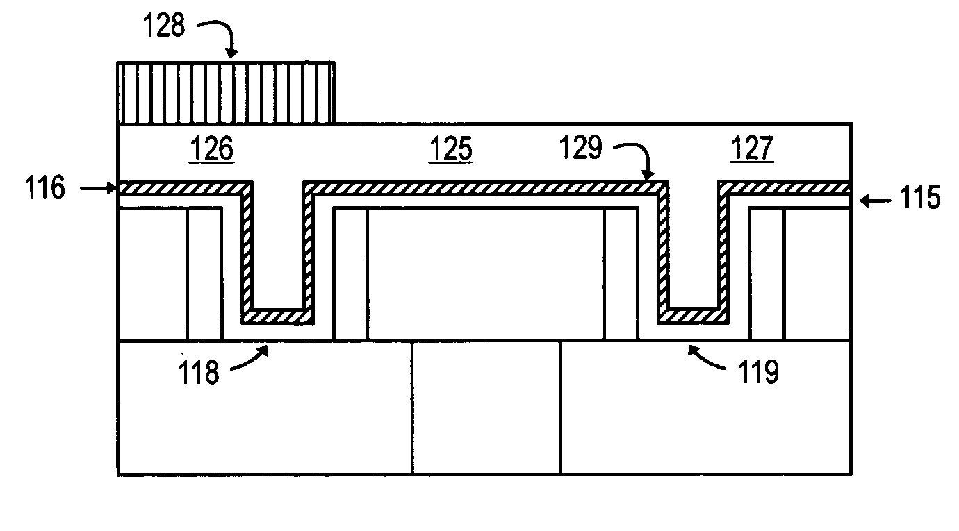
[0013]FIGS. 1a–1f illustrate structures that may be formed, when carrying out an embodiment of the method of the present invention. FIG. 1a re...


PUM

PropertyMeasurementUnit
temperatureaaaaaaaaaa
workfunctionaaaaaaaaaa

Abstract

A method for making a semiconductor device is described. That method comprises forming a first dielectric layer on a substrate, then forming a trench within the first dielectric layer. After forming a second dielectric layer on the substrate, a first metal layer is formed within the trench on a first part of the second dielectric layer. A second metal layer is then formed on the first metal layer and on a second part of the second dielectric layer.

Description

FIELD OF THE INVENTION[0001]The present invention relates to methods for making semiconductor devices, in particular, semiconductor devices that include metal gate electrodes.BACKGROUND OF THE INVENTION[0002]MOS field-effect transistors with very thin gate dielectrics made from silicon dioxide may experience unacceptable gate leakage currents. Forming the gate dielectric from certain high-k dielectric materials, instead of silicon dioxide, can reduce gate leakage. Because, however, such a dielectric may not be compatible with polysilicon, it may be desirable to use metal gate electrodes in devices that include high-k gate dielectrics.[0003]When making a CMOS device that includes metal gate electrodes, a replacement gate process may be used to form gate electrodes from different metals. In that process, a first polysilicon layer, bracketed by a pair of spacers, is removed to create a trench between the spacers. The trench is filled with a first metal. A second polysilicon layer is th...

Claims


Application Information

Patent Timeline
Patent Type & Authority Patents(United States)
IPC IPC(8): H01L21/44H01L21/8234H01L21/8238
CPCH01L21/82345H01L29/66545H01L21/823842H01L21/28229H01L29/513H01L29/517H01L27/092
Inventor BRASK, JUSTIN K.KAVALIEROS, JACKDOCZY, MARK L.SHAH, UDAYBARNS, CHRIS E.METZ, MATTHEW V.DATTA, SUMANCAPPELLANI, ANNALISACHAU, ROBERT S.
Owner INTEL CORP
Why Eureka
Try Eureka