Delay locked loop in semiconductor memory device and locking method thereof

a technology of semiconductor memory and lock loop, which is applied in the direction of digital storage, pulse automatic control, instruments, etc., can solve the problems of clock divider operation, delay time between external clock and internal clock,

Inactive Publication Date: 2006-12-26
SK HYNIX INC
View PDF5 Cites 34 Cited by
  • Summary
  • Abstract
  • Description
  • Claims
  • Application Information

AI Technical Summary

Problems solved by technology

When an external clock is used for an internal circuit, a delay time between the external clock and an internal clock inevitably occurs due to the internal circuit.
The problem due to generation of the short pulse is that the operation of the clock dividers 114 and 117 dose not be performed simultaneously.

Method used


Image

  • Delay locked loop in semiconductor memory device and locking method thereof
  • Delay locked loop in semiconductor memory device and locking method thereof
  • Delay locked loop in semiconductor memory device and locking method thereof

Examples


Embodiment Construction

[0027]Hereinafter, a delay locked loop (DLL) for use in a semiconductor device in accordance with the present invention will be described in detail referring to the accompanying drawings.

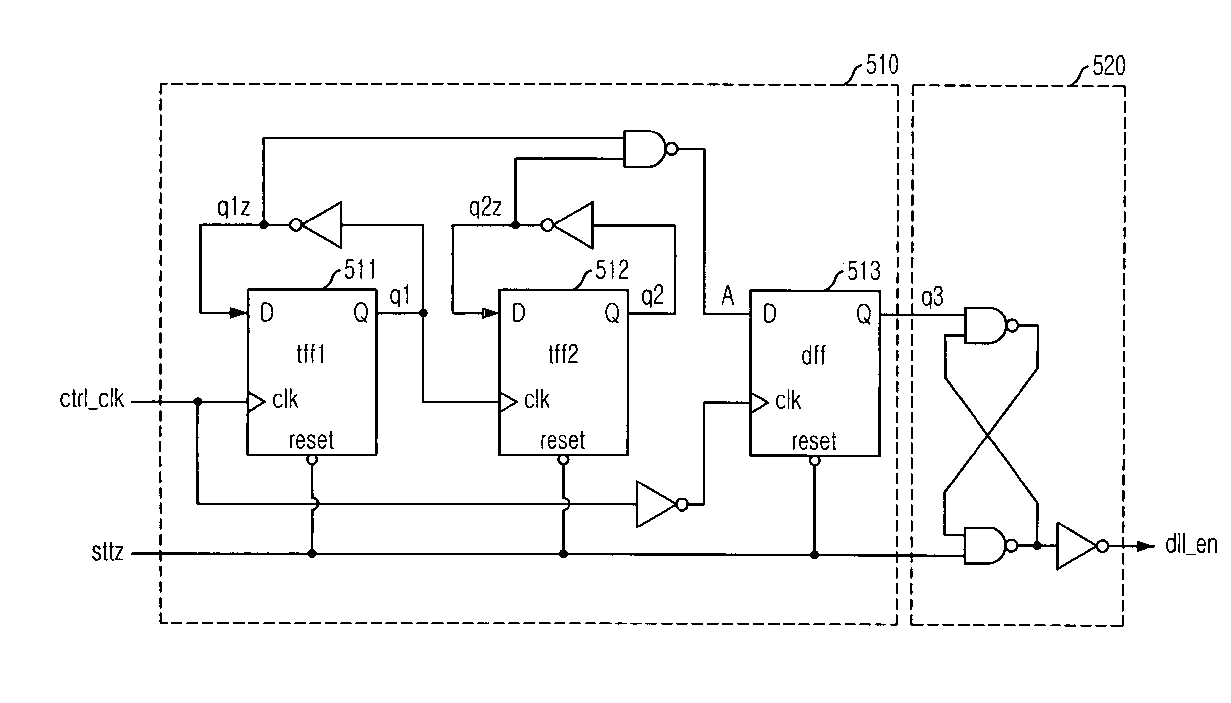
[0028]FIG. 5 is a block diagram of a DLL controller in accordance with a preferred embodiment of the present invention. The DLL controller includes a plurality of T flip-flop blocks 511 and 512, a D flip-flop 513 and a latch unit 520. The plurality T flip-flops 511 and 512 activate an enable signal dll_en at a falling edge of a control clock signal ctr_clk inputted from a second clock buffer (not shown) by using the control clock signal ctr_clk and a reset bar signal sttz. Herein, the reset bar signal is used for resetting the DLL controller.

[0029]In detail, a first T flip-flop 511 receives the control signal ctrl_clk as a clock and changes its state whenever a clock pulse of the control signal ctrl_clk is inputted. That is, as shown in FIG. 7, the first T flip-flop 511 divides the control clock by ...


PUM


Abstract

Provided is a delay locked loop (DLL) adapted for high-speed operation of a semiconductor memory device. The delay locked loop (DLL) includes: a clock buffer; a plurality of clock dividers; and a controller for activating an enable signal at a falling edge of a control clock by using a reset bar signal and a control clock outputted from the clock buffer.

Description

FIELD OF INVENTION[0001]The present invention relates to a semiconductor memory device; and, more particularly, to a delay locked loop (DLL) of a semiconductor memory device adapted for high-speed operation.DESCRIPTION OF PRIOR ART[0002]In systems or circuits, a clock is used as a reference for adjusting an operational timing and is also used for securing high-speed and error-free operation in the system or the circuit. When an external clock is used for an internal circuit, a delay time between the external clock and an internal clock inevitably occurs due to the internal circuit. The delay time is called a clock skew. Therefore, in order to compensate for the delay time and make the internal clock have the same phase as that of the external clock, a delay locked loop (hereinafter, referred to as a DLL) is typically used in the semiconductor memory device. That is, the DLL synchronizes the external clock with an internal clock.[0003]FIG. 1 is a block diagram of a prior art DLL for ...

Claims


Application Information

Patent Timeline
Patent Type & Authority Patents(United States)
IPC IPC(8): H03L7/06G11C11/40H03L7/081H03L7/10
CPCH03L7/0814H03L7/10G11C11/40
Inventor LIM, MIN-SU
Owner SK HYNIX INC
Why Eureka
Try Eureka