Liquid crystal display panel with static electricity prevention circuit

a technology of static electricity prevention and which is applied in the direction of electrical testing, measurement devices, instruments, etc., can solve the problem that the test pad part of the related art does not effectively protect the thin film transistor inside the liquid crystal display panel, and achieve the effect of preventing static electricity flowing through the pad par

Inactive Publication Date: 2006-12-26
LG DISPLAY CO LTD
View PDF9 Cites 9 Cited by
  • Summary
  • Abstract
  • Description
  • Claims
  • Application Information

AI Technical Summary

Benefits of technology

[0029]Accordingly, it is an advantage of the present invention to provide a static electricity prevention type liquid crystal display panel for preventing static electricity flowing through a pad part.
[0030]Additional features and advantages of the invention will be set forth in the description that follows, and in part will be apparent from the description, or may be learned by practice of the invention. These and other advantages of the invention will be realized and attained by the structure particularly pointed out in the written description and claims hereof, as well as the appended drawings.
[0031]In order to achieve these and other advantages of the invention, a static electricity prevention type liquid crystal display panel according to an aspect of the present invention includes a picture display part having a plurality of liquid crystal cells; a signal pad part for applying a driving signal to be inputted to signal lines of the picture display part, wherein the signal pad part includes a plurality of pads connected to respective ones of the signal lines; and a static electricity prevention circuit having a thin film transistor with a floating gate for connecting at least one of said pads with an equipotential line in the presence of static electricity.
[0032]Herein, the static electricity prevention circuit causes the pad to be insulated from the shorting bar and the other pads, when a normal drive signal is applied to the pad, so as to apply the drive signal to the signal lines of the picture display part.
[0033]The static electricity prevention circuit includes a first capacitor connected between the floating gate and a first terminal of the thin film transistor connected to the shorting bar; and a second capacitor connected between the floating gate and a second terminal of the thin film transistor connected to the pad.
[0034]The liquid crystal display further includes a second static electricity prevention circuit formed between the pad and a first and a second drive voltage supply line for bypassing the static electricity flowing into the pad to the first and second drive voltage supply lines.

Problems solved by technology

In this way, the test pad part of the related art does not effectively protect the thin film transistor inside the liquid crystal display panel from the static electricity flowing into the test pad in the fabricating process and the inspection process of the liquid crystal display panel even though the test pad is connected to the first and second drive voltage supply lines VDDL and VSSL.

Method used


Image

  • Liquid crystal display panel with static electricity prevention circuit
  • Liquid crystal display panel with static electricity prevention circuit
  • Liquid crystal display panel with static electricity prevention circuit

Examples


first embodiment

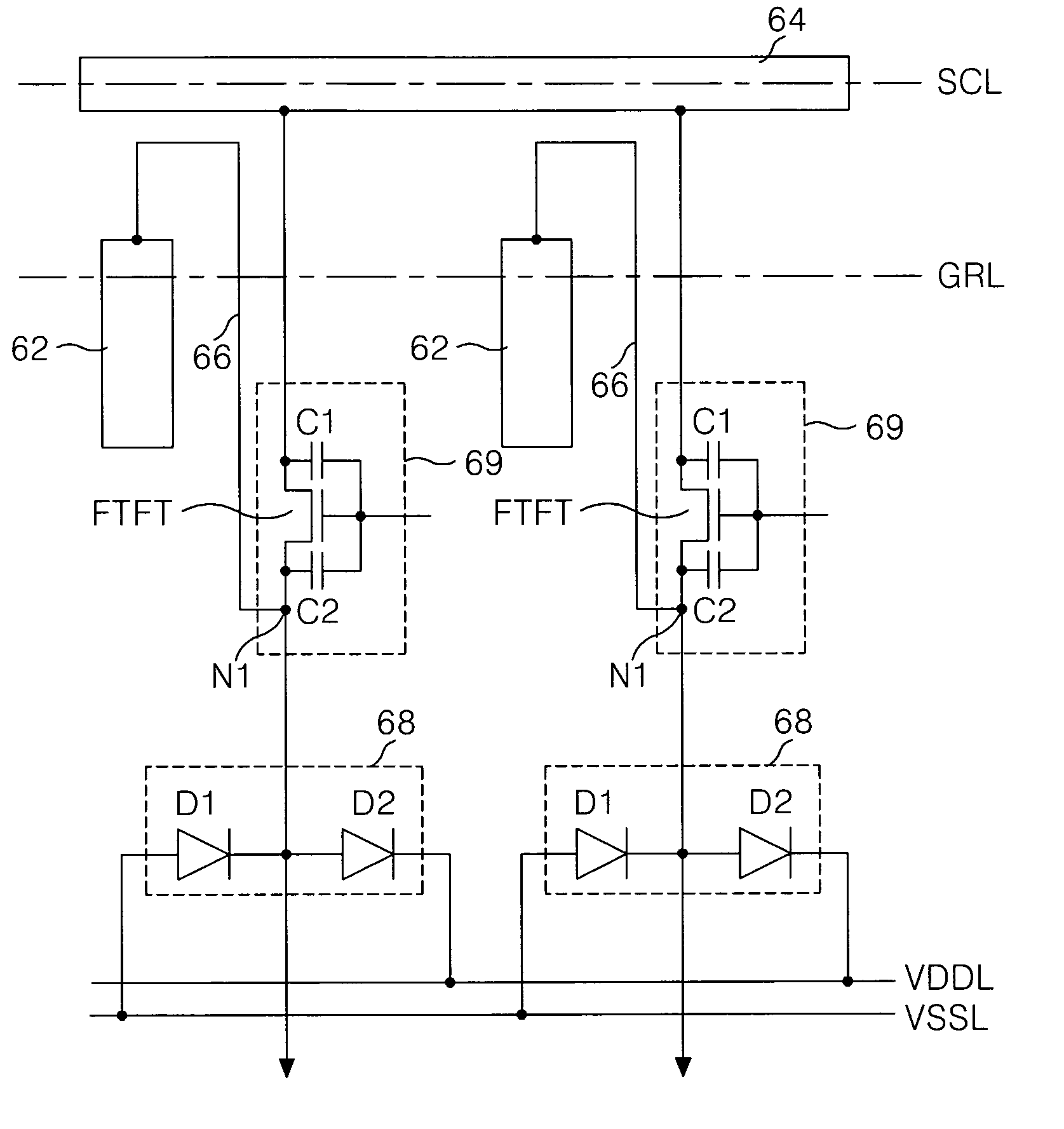
[0058]FIG. 6 illustrates a test pad part of a liquid crystal display panel for preventing static electricity according to the present invention.

[0059]Referring to FIG. 6, the test pad part includes a plurality of test pads 62, a first static electricity prevention circuit 68 connected between each test pad 62 and a first and a second drive voltage supply lines VDDL and VSSL, and a second static electricity prevention circuit 69 connected between each test pad 62 and a shorting bar 64.

[0060]The test pads 62 are connected to signal lines of a picture display part (not shown). The test pads 62 are used to apply a test signal during inspection processes such as a lighting-up test of the liquid crystal display panel, and at the same time to apply a bias voltage in an aging process for stabilizing the liquid crystal display panel.

[0061]The first static electricity prevention circuit 68 is connected between the test pad 62 and the first and second drive voltage supply lines VSSL and VDDL. ...

third embodiment

[0080]FIG. 9 illustrates a test pad part of a static electricity prevention type liquid crystal display panel according to the present invention.

[0081]The test pad part illustrated in FIG. 9 includes the same components as the test pad part shown in FIG. 8A, except that a current limit resistor R is formed between a first static electricity prevention circuit 98 and signal lines of the picture display part (not shown) instead of between the first and second static electricity prevention circuits 88 and 89.

[0082]The test pads 92 are connected to the signal lines of the picture display part (not shown). The test pads 92 are used to apply a test signal in inspection processes such as a lighting-up test of the liquid crystal display panel, and at the same time to apply a bias voltage in an aging process for stabilizing the liquid crystal display panel.

[0083]The first static electricity prevention circuit 98 is connected between the test pad 92 and the first and second drive voltage supp...

fourth embodiment

[0092]FIG. 10 illustrates a test pad part of a static electricity prevention type liquid crystal display panel according to the present invention.

[0093]The test pad part 102 in FIG. 10 includes the same components as the test pad part shown in FIG. 6 except that a test pad 102 is connected to a shorting bar 104 through a resistor R, as well as a second static electricity prevention circuit 109.

[0094]The test pads 102 are connected to the signal lines of the picture display part (not shown). The test pads 102 are used to apply a test signal in inspection processes such as a lighting-up test of the liquid crystal display panel, and at the same time to apply a bias voltage in an aging process for stabilizing the liquid crystal display panel.

[0095]The first static electricity prevention circuit 108 is connected between the test pad 102 and the first and second drive voltage supply lines VSSL and VDDL. More specifically, the first static electricity prevention circuit 108 includes a firs...


PUM

PropertyMeasurementUnit
drive voltageaaaaaaaaaa
resistanceaaaaaaaaaa

Abstract

The present invention relates to a static electricity prevention type liquid crystal display panel for preventing static electricity flowing in through a pad part. A static electricity prevention type liquid crystal display panel according to an embodiment of the present invention includes a picture display part having a plurality of liquid crystal cells; a signal pad part applying a drive signal to be inputted to signal lines of the picture display part, and wherein the signal pad part includes a plurality of pads connected to the signal lines; and a static electricity prevention circuit having a thin film transistor with a floating gate for connecting the pad with a shorting bar by a static electricity flowing into the pad for the pad to form an equipotential with respect to the static electricity.

Description

[0001]This application claims the benefit of Korean Patent Application No. 2002-47867, filed on Aug. 13, 2002, which is hereby incorporated by reference for all purposes as if fully set forth herein.BACKGROUND OF THE INVENTION[0002]1. Field of the Invention[0003]The present invention relates to a liquid crystal display panel, and more particularly to a static electricity prevention type liquid crystal display panel that is adaptive for preventing static electricity from flowing through a pad part.[0004]2. Discussion of the Related Art[0005]A general liquid crystal display device displays pictures by controlling light transmittance of liquid crystal using an electric field. To this end, the liquid crystal display device includes a liquid crystal display panel, where liquid crystal cells are arranged in a matrix, and a drive circuit for driving the liquid crystal display panel.[0006]The liquid crystal display panel includes a thin film transistor array substrate and a color filter arr...

Claims


Application Information

Patent Timeline
Patent Type & Authority Patents(United States)
IPC IPC(8): G02F1/1333G01R31/00G02F1/133G02F1/1345G02F1/1362G09G3/20G09G3/36H01L29/786
CPCG02F1/136204G02F1/133
Inventor KIM, BYEONG KOOHA, YONG MINHWANG, HAN WOOK
Owner LG DISPLAY CO LTD
Why Eureka
Try Eureka