Semiconductor die package including carrier with mask and semiconductor die

a technology of semiconductor die and carrier, which is applied in the direction of semiconductor/solid-state device details, semiconductor devices, electrical apparatus, etc., can solve the problems of solder ball collapse and loss of shape, more performance limitation factors of conventional packages, and increase the cost and processing time of the packag

Inactive Publication Date: 2007-01-02
FAIRCHILD SEMICON CORP +1
View PDF18 Cites 130 Cited by
  • Summary
  • Abstract
  • Description
  • Claims
  • Application Information

AI Technical Summary

Problems solved by technology

However, for the most part, decades-old package technology is often used to package semiconductor dies.
Advances in semiconductor processing technology, however, have made the parasitics associated with conventional packages more of a performance-limiting factor.
A full reflow process is not performed, since performing a full reflow process causes the solder balls to collapse and lose their shape.
For example, using two separate steps to place solder balls on the semiconductor die and the carrier increases the cost and the processing time for the package.
In addition, using two steps to place solder balls on the semiconductor die and the carrier can increase the likelihood that the bumps on the two components will not be coplanar.
Moreover, because the solder balls on the carrier are partially reflowed, the bonds formed between the solder balls and the carrier are weaker than if a full reflow process were performed.

Method used


Image

  • Semiconductor die package including carrier with mask and semiconductor die
  • Semiconductor die package including carrier with mask and semiconductor die
  • Semiconductor die package including carrier with mask and semiconductor die

Examples


Embodiment Construction

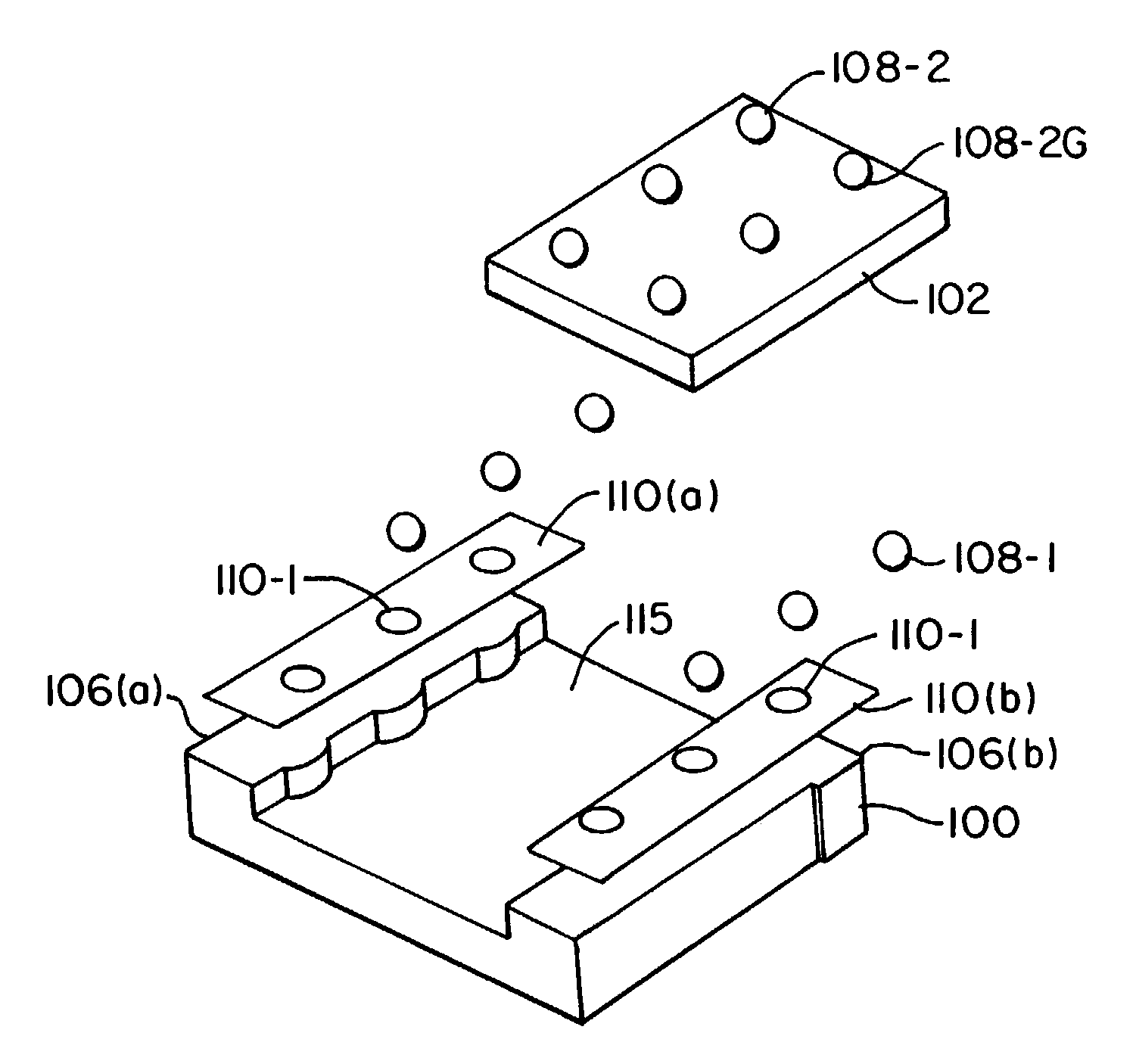
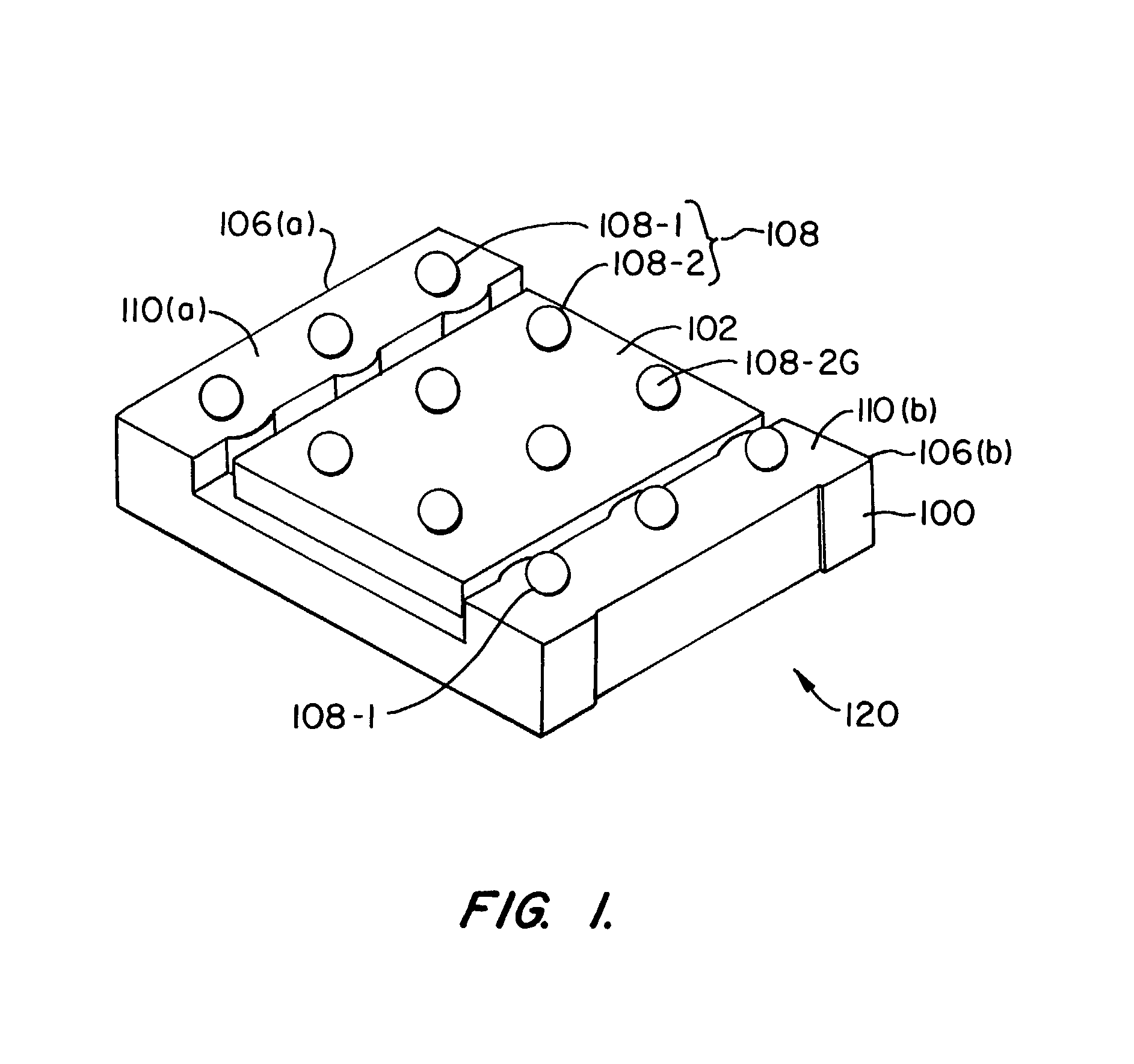
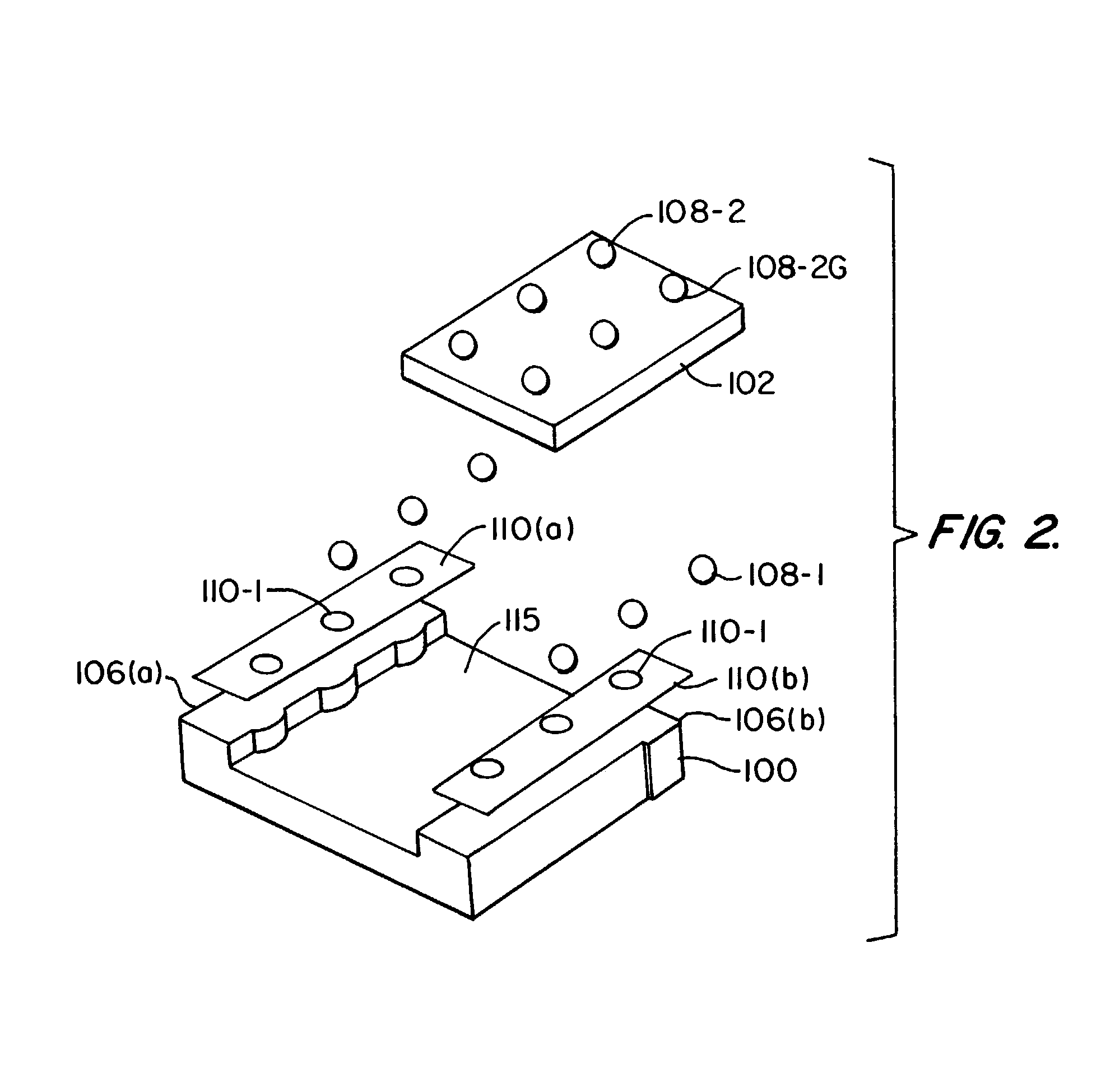
[0022]One embodiment of the invention is directed to a carrier comprising a die attach region and a plurality of edge regions. Each edge region can have a surface that is elevated with respect to the die attach region. Each edge region can also partially define the die attach region. The carrier may also comprise a base metal and one or more layers of material on the base metal. A first solder mask having one or more apertures is disposed on an edge region.

[0023]A semiconductor die is attached to the die attach region of the carrier. In some embodiments, the semiconductor die may have a MOSFET with a source region, a gate region, and a drain region. When the semiconductor die is attached to the die attach region of the carrier, the drain region is proximate to the die attach region and the source region is distal to the die attach region.

[0024]A second solder mask can be disposed on the semiconductor die. The second solder mask may comprise, for example, a silicon nitride layer with...


PUM


Abstract

A carrier for use in a semiconductor die package is disclosed. In one embodiment, the carrier includes a die attach region and an edge region. A solder mask is on the edge region.

Description

CROSS-REFERENCES TO RELATED APPLICATIONS[0001]This application is a divisional of U.S. patent application Ser. No. 09 / 841,333, filed on Apr. 23, 2001 now U.S. Pat. No. 6,645,791. This application is herein incorporated by reference for all purposes.BACKGROUND OF THE INVENTION[0002]Silicon process technology has advanced significantly in the past decade. However, for the most part, decades-old package technology is often used to package semiconductor dies. In a conventional packaging process, gold wires couple a semiconductor die and a lead frame together in a semiconductor die package. Leads in the lead frame are coupled to the conductive lands on a circuit substrate such as a printed circuit board (PCB).[0003]Advances in semiconductor processing technology, however, have made the parasitics associated with conventional packages more of a performance-limiting factor. This is particularly true in the case of power switching devices where, as in the case of power metal oxide field eff...

Claims


Application Information

Patent Timeline
Patent Type & Authority Patents(United States)
IPC IPC(8): H01L23/12H01L23/52H01L21/48H01L21/68H01L23/13H01L23/498
CPCH01L21/4853H01L21/568H01L21/6835H01L23/13H01L23/49816H01L24/11H01L2924/1306H01L2924/13091H01L2924/00H01L2924/12042H01L2224/05573H01L2224/05548H01L2224/056H01L24/05H01L2924/00014
Inventor NOQUIL, JONATHAN A.ESTACIO, MARIA C.
Owner FAIRCHILD SEMICON CORP
Why Eureka
Try Eureka