Electronic component-mounted structure, method for mounting electronic component, electro-optical device, and electronic apparatus

a technology of electronic components and mounting methods, applied in the direction of dielectric characteristics, printed circuit aspects, association of printed circuit non-printed electric components, etc., can solve the problems of increasing production costs, difficult to secure elastic deformation of conductive particles, and increasing production costs, so as to and improve the reliability of electrical connections.

Active Publication Date: 2007-01-09
BOE TECH GRP CO LTD
View PDF6 Cites 22 Cited by
  • Summary
  • Abstract
  • Description
  • Claims
  • Application Information

AI Technical Summary

Benefits of technology

[0009]An advantage of the invention is that it provides an electronic component-mounted structure and a method for mounting an electronic component in which reliability of electrical connection can be improved. Another advantage of the invention is that it provides an electro-optical device and an electronic apparatus each having excellent reliability of electrical connection.
[0010]According to an aspect of the invention, an electronic component-mounted structure includes an electronic component having a bump electrode, the bump electrode including a projection made of a first resin and a conductive film covering at least a top of the projection; a substrate having a connecting terminal; and a second resin filling the space between the electronic component and the substrate, wherein the bump electrode abuts against the connecting terminal, and wherein the relationship T0<Tgr<Tgb is satisfied, where T0 is an operating temperature of the electronic component mounted on the substrate, Tgb is a glass transition temperature of the first resin, and Tgr is a glass transition temperature of the second resin.
[0011]In particular, preferably, the relationship αb1<αr1 is satisfied, where αb1 is a thermal expansion coefficient of the first resin below the glass transition temperature Tgb, and αrb1 is a thermal expansion coefficient of the second resin below the glass transition temperature Tgr.
[0012]In these constructions, since the conductive contact between the bump electrode and the connecting terminal can be ensured, it is possible to improve reliability of electrical connection.
[0013]Furthermore, when the relationship T0<Tgr<Tc<Tgb is satisfied, where Tc is a curing temperature of the second resin, preferably, the relationship αb1(Tc−T0)<αr2(Tc−Tgr)+αr1(Tgr−T0) is satisfied, where αb1 is a thermal expansion coefficient of the first resin below the glass transition temperature Tgb, αr2 is a thermal expansion coefficient of the second resin above the glass transition temperature Tgr, and αr1 is a thermal expansion coefficient of the second resin below the glass transition temperature Tgr.
[0014]Furthermore, when the relationship T0<Tgr<Tgb<Tc is satisfied, where Tc is a curing temperature of the second resin, preferably, the relationship αb2(Tc−Tgb)+αb1(Tgb−T0 )<αr2(Tc−Tgr)+αr1(Tgr−T0 ) is satisfied, where αb2 is a thermal expansion coefficient of the first resin above the glass transition temperature Tgb, αb1 is a thermal expansion coefficient of the first resin below the glass transition temperature Tgb, αr2 is a thermal expansion coefficient of the second resin above the glass transition temperature Tgr, and αr1 is a thermal expansion coefficient of the second resin below the glass transition temperature Tgr.

Problems solved by technology

However, the conductive particles 22a having a small particle size have high rigidity and it is difficult to secure elastic deformation of the conductive particles 22a that is sufficient for improving reliability of electrical connection.
Consequently, the cost of the anisotropic conductive film 22 has increased, resulting in an increase in production cost.
It has also become more difficult to secure sufficient elastic deformation of the conductive particles 22a, resulting in a difficulty in securing reliability of electrical connection against a change in temperature.
Additionally, in the method in which conductive particles composed of conductive rubber are used, it is still more difficult to decrease the particle size.

Method used


Image

  • Electronic component-mounted structure, method for mounting electronic component, electro-optical device, and electronic apparatus
  • Electronic component-mounted structure, method for mounting electronic component, electro-optical device, and electronic apparatus
  • Electronic component-mounted structure, method for mounting electronic component, electro-optical device, and electronic apparatus

Examples


Embodiment Construction

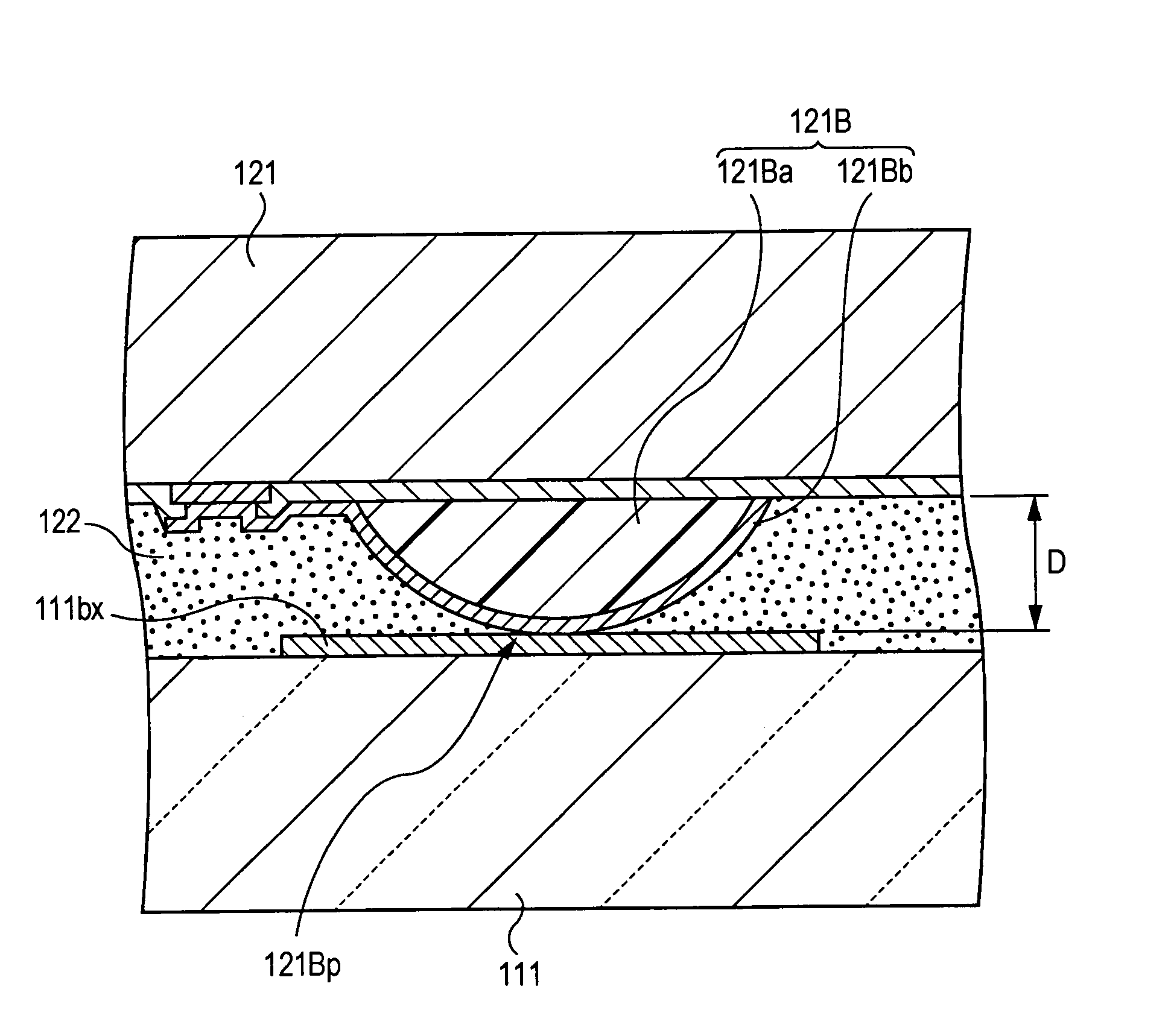
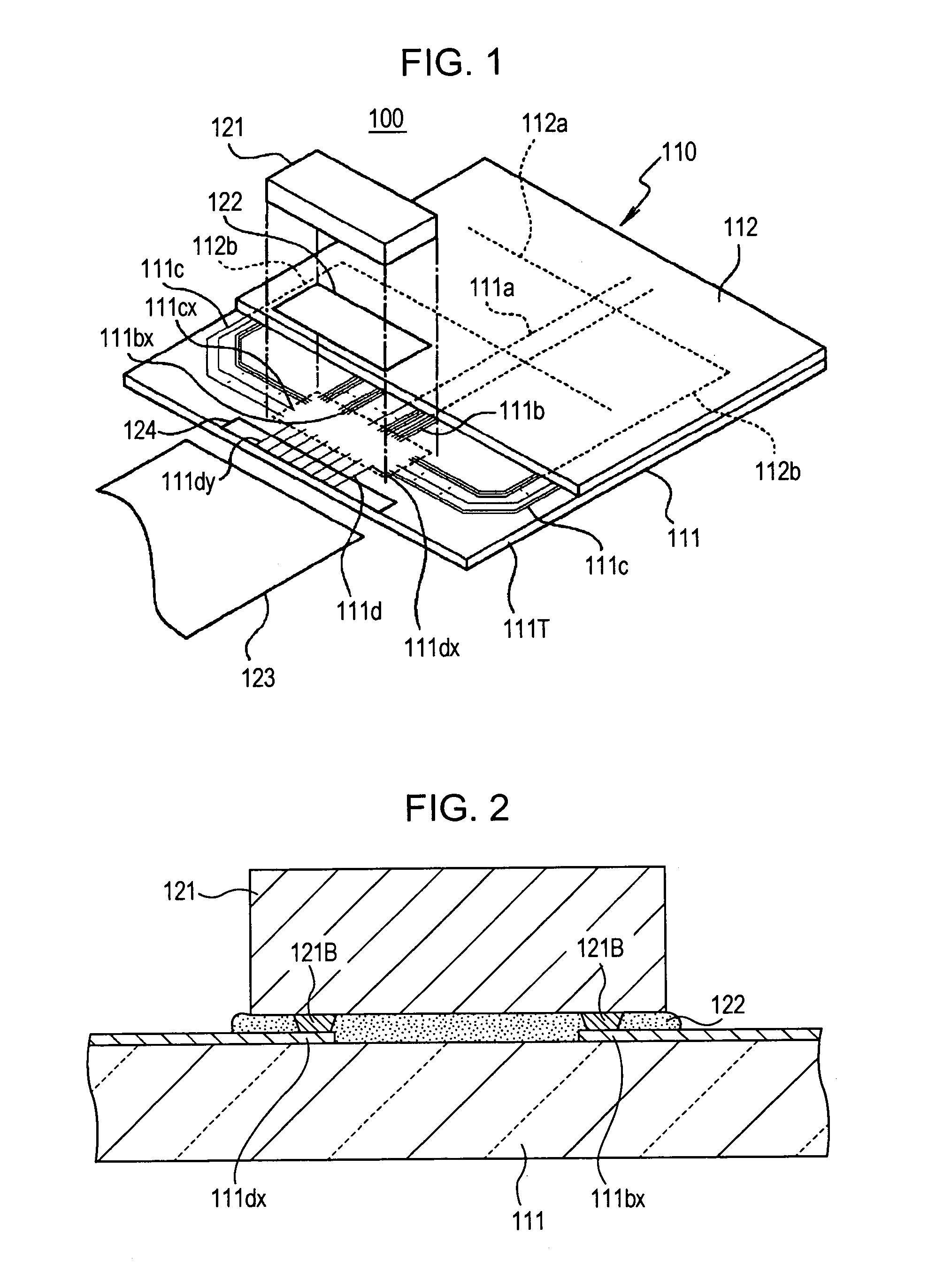
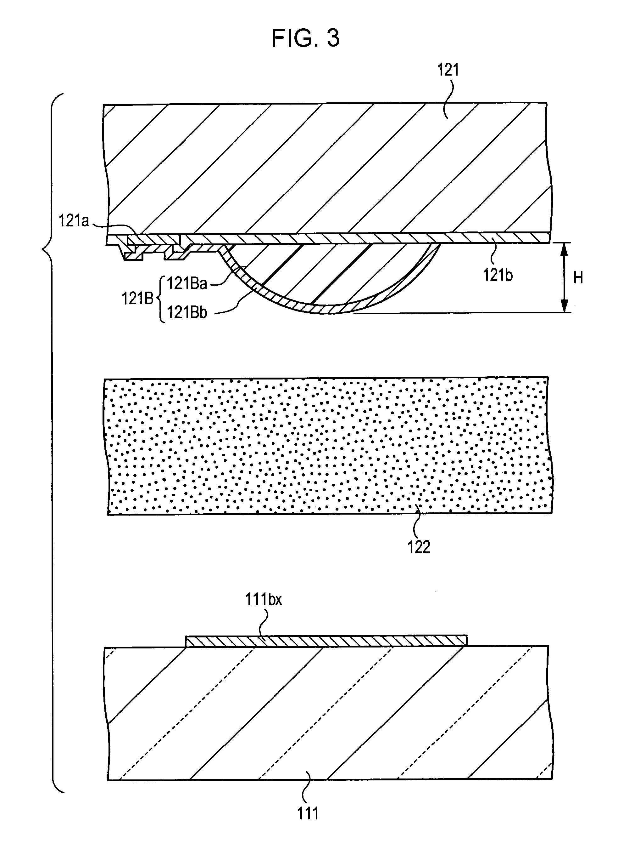
[0035]Embodiments of the invention will be described below with reference to the drawings. In the drawings, the scale for each element is varied appropriately so that the element is of a recognizable size.

[Electro-Optical Device]

[0036]FIG. 1 is an assembly view of an electro-optical device according to an embodiment of the invention. A liquid crystal device 100 shown in FIG. 1 includes a liquid crystal panel 110 and an electronic component (IC chip for driving liquid crystal) 121. Furthermore, according to need, the liquid crystal device 100 is appropriately provided with additional elements, such as a polarizer, a reflector sheet, and a backlight, (not shown).

[0037]The liquid crystal panel 110 includes substrates 111 and 112 which are composed of glass, plastic, or the like. The substrates 111 and 112 are arranged so as to be opposed to each other, and are bonded to each other with a sealant or the like (not shown). A liquid crystal which is an electro-optical substance (not shown)...


PUM


Abstract

An electronic component-mounted structure includes an electronic component having a bump electrode, the bump electrode including a projection made of a first resin and a conductive film covering at least a top of the projection; a substrate having a connecting terminal; and a second resin filling the space between the electronic component and the substrate, wherein the bump electrode abuts against the connecting terminal, and wherein the relationship T0<Tgr<Tgb is satisfied, where T0 is an operating temperature of the electronic component mounted on the substrate, Tgb is a glass transition temperature of the first resin, and Tgr is a glass transition temperature of the second resin.

Description

RELATED APPLICATIONS[0001]This application claims priority to Japanese Patent Application No. 2004-274625 filed Sep. 22, 2004 which is hereby expressly incorporated by reference herein in its entirety.BACKGROUND OF THE INVENTION[0002]1. Technical Field[0003]The present invention relates to electronic component-mounted structures; methods for mounting electronic components; electro-optical devices, such as liquid crystal devices and light-emitting devices, e.g., organic electro-luminescence (EL) devices, and inorganic EL devices; and electronic apparatuses.[0004]2. Related Art[0005]In circuit boards and liquid crystal display devices mounted on various types of electronic apparatuses, techniques for mounting electronic components, such as semiconductor ICs, are used. For example, in a liquid crystal display device, an IC chip for driving liquid crystal, which drives a liquid crystal panel, is mounted. The IC chip for driving liquid crystal may be directly mounted on a glass substrate...

Claims


Application Information

Patent Timeline
Patent Type & Authority Patents(United States)
IPC IPC(8): H01L23/48H01L23/52H01L29/40
CPCH01L21/563H01L24/10H01L24/13H01L24/29H01L24/83H01L24/90H05K3/325H01L2924/12041H01L2224/81191H01L2224/32225H01L2924/0665H01L2924/01043H01L2924/01023H01L2924/01006H01L2224/2919H01L33/62H01L2224/13099H01L2224/16225H01L2224/73203H01L2224/73204H01L2224/83101H01L2224/83856H01L2924/01005H01L2924/01013H01L2924/01015H01L2924/01029H01L2924/01033H01L2924/01049H01L2924/0105H01L2924/01074H01L2924/01078H01L2924/01079H01L2924/01082H01L2924/14H05K3/305H05K2201/0133H05K2201/0367H05K2201/068H05K2201/10977H01L2924/00H01L2924/00012H01L24/02H01L24/05H01L24/11H01L24/16H01L24/81H01L2224/05001H01L2224/05124H01L2224/05548H01L2224/05644H01L2224/05647H01L2224/05655H01L2224/13H01L2224/13008H01L2224/1319H01L2924/0001H01L2924/00014H01L2224/02H05K1/18H05K3/30
Inventor SAITO, ATSUSHI
Owner BOE TECH GRP CO LTD
Why Eureka
Try Eureka