CMOS power on reset circuit

a technology of power on and reset circuit, applied in the direction of pulse automatic control, pulse technique, electronic switching, etc., can solve problems such as device not working properly, and achieve the effect of less sensitive to processing and creating hysteresis

Active Publication Date: 2007-01-09
XILINX INC
View PDF10 Cites 44 Cited by
  • Summary
  • Abstract
  • Description
  • Claims
  • Application Information

AI Technical Summary

Benefits of technology

[0010]When the IC device is powered-on, the POR circuit asserts the reset signal, which in turn can be used to reset the device to a known state. As the supply voltage increases, the tracking node voltage charges through the pull-up resistor and tracks the supply voltage. In response thereto, the buffer circuit asserts the reset signal to logic high. When the supply voltage reaches a predetermined power-up reset level, the pull-down transistor turns on and discharges the tracking node toward ground potential. In response thereto, the buffer circuit de-asserts the reset signal to logic low, which in turn can be used to terminate the reset operation. During device power-down, the reset signal is initially de-asserted to logic low. When the supply voltage decreases below a predetermined power-down reset level, the pull-down transistor turns off and allows the tracking node to charge through the pull-up resistor, which in turn causes the buffer circuit to assert the reset signal to logic high. The asserted logic high reset signal can be used to reset the device to a known state before power is lost.
[0011]Because the pull-down transistor is controlled by a ratioed voltage created by the voltage divider circuit in response to the supply voltage, the power-up and power-down reset levels can be adjusted by manipulating the relative resistances in the voltage divider circuit. This is advantageous because process and temperature variations typically affect the resistors in the voltage divider circuit similarly, and therefore cancel each other when determining the ratioed voltage. In this manner, the power-up and power-down reset levels can be set to predetermined multiples of the threshold voltage VTN of the pull-down transistor, and are less sensitive to process and temperature variations.
[0012]For some embodiments, the voltage divider circuit includes a shunt transistor that can be used to increase or decrease the ratioed voltage to create hysteresis between the power-up and power-down reset levels.

Problems solved by technology

For example, if one or more latches power-up into an undesirable state, the device may not function properly.

Method used


Image

  • CMOS power on reset circuit
  • CMOS power on reset circuit
  • CMOS power on reset circuit

Examples


Embodiment Construction

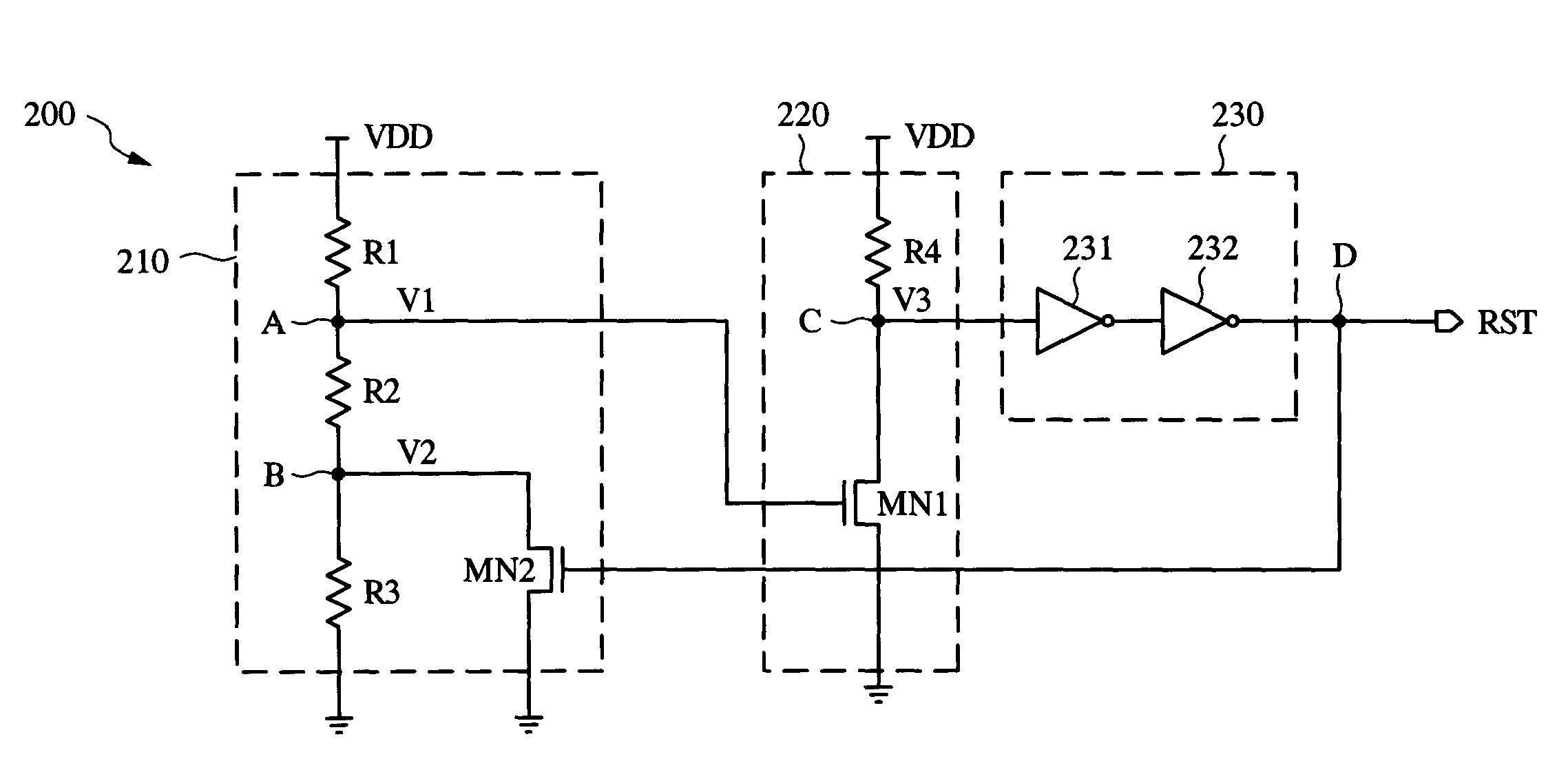
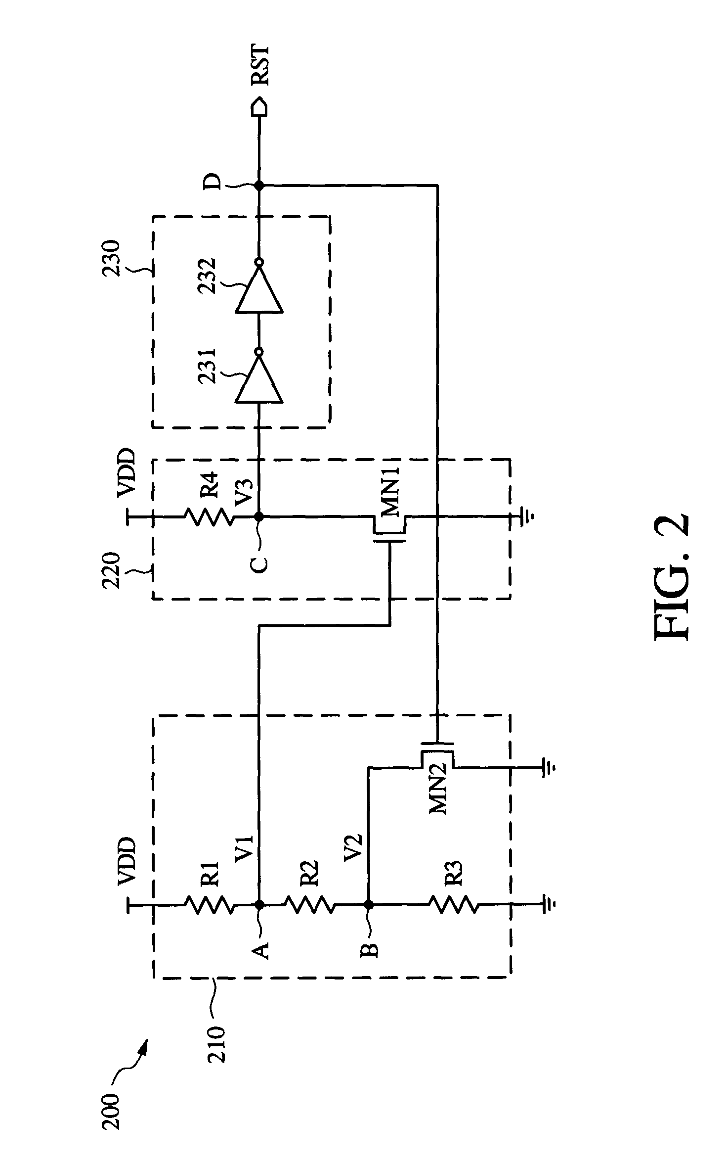
[0020]The present invention is applicable to a variety of integrated circuits and systems. The present invention has been found to be particularly applicable and beneficial for providing reset signals during power-up and power-down operations for programmable logic devices, although embodiments of the present invention are equally applicable to other circuits and devices. In the following description, for purposes of explanation, specific nomenclature is set forth to provide a thorough understanding of the present invention. In other instances, well-known circuits and devices are shown in block diagram form to avoid obscuring the present invention. Further, the logic levels assigned to various signals in the description below are arbitrary, and thus can be modified (e.g., reversed polarity) as desired. Accordingly, the present invention is not to be construed as limited to specific examples described herein but rather includes within its scope all embodiments defined by the appended...


PUM


Abstract

A power-on reset circuit for generating a reset signal for an associated IC device includes a pull-up resistor connected between a supply voltage and a tracking node, a pull-down transistor connected between the tracking node and ground potential, and a voltage divider circuit connected between the supply voltage and ground potential. The voltage divider circuit has a first ratioed voltage node coupled to the gate of the pull-down transistor. For some embodiments, the voltage divider circuit includes a first resistor connected between the voltage supply and the first ratioed voltage node, a second resistor connected between the first ratioed voltage node and a second ratioed voltage node, a third resistor connected between the second ratioed voltage node and ground potential, and a shunt transistor connected between the second ratioed voltage node and ground potential has a gate responsive to the reset signal.

Description

FIELD OF INVENTION[0001]The present invention relates generally to integrated circuits, and more specifically to power-on reset circuits.DESCRIPTION OF RELATED ART[0002]When an integrated circuit (IC) device is powered on, it is important that the device's internal logic is set to a known state to ensure proper operation. For example, if one or more latches power-up into an undesirable state, the device may not function properly. Thus, most IC devices include a power-on reset (POR) circuit that asserts a reset signal when a supply voltage is detected and then de-asserts the reset signal when the supply voltage has reached an acceptable level that is sufficient for the device's normal operation. When asserted, the reset signal is typically used to reset the device's internal logic to a known state. When de-asserted, the reset signal is typically used to terminate the reset operation and allow the device to commence normal operation. The POR circuit can also be used to assert the rese...

Claims


Application Information

Patent Timeline
Patent Type & Authority Patents(United States)
IPC IPC(8): H03L7/00
CPCH03K17/223
Inventor ZHOU, SHI-DONGHUANG, GUBO
Owner XILINX INC
Why Eureka
Try Eureka