

Microwave transmission line having dielectric film layers providing negative space charge effects
a dielectric film and negative space charge technology, applied in the direction of waveguides, semiconductor devices, semiconductor/solid-state device details, etc., can solve the problems of difficult to realize a low-loss microwave transmission line, the substrate has a significantly reduced resistivity in the vicinity of its top surface, and the czochralski method has a resistivity of 100 cm or less, so as to prevent the increase of transmission loss and maintain long-term stability
- Summary
- Abstract
- Description
- Claims
- Application Information
AI Technical Summary
Benefits of technology
Problems solved by technology
Method used
Image

Examples
embodiment 1
[0037](Embodiment 1)
[0038]A first embodiment of the present invention will be described hereinafter with reference to the drawings.
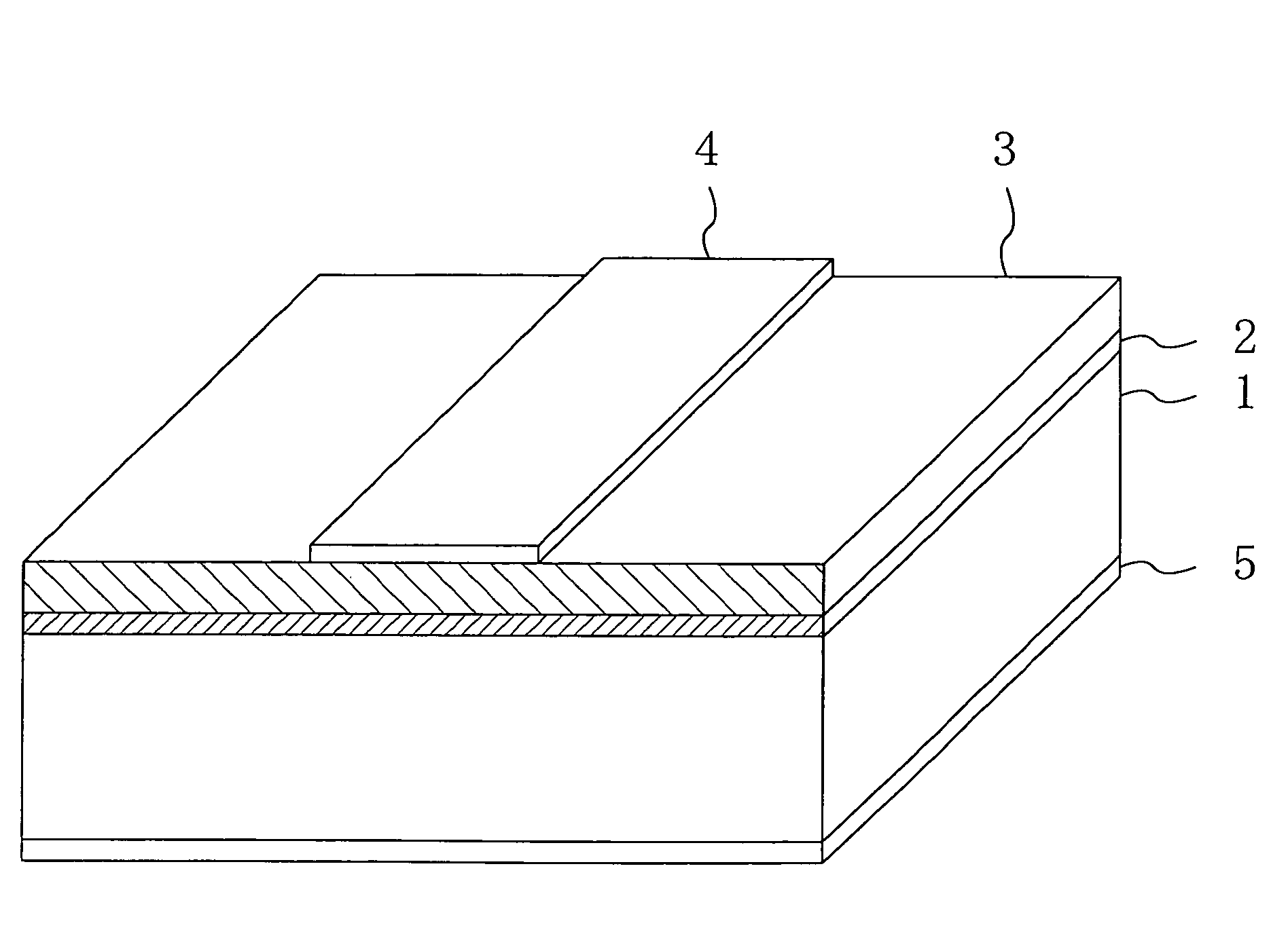
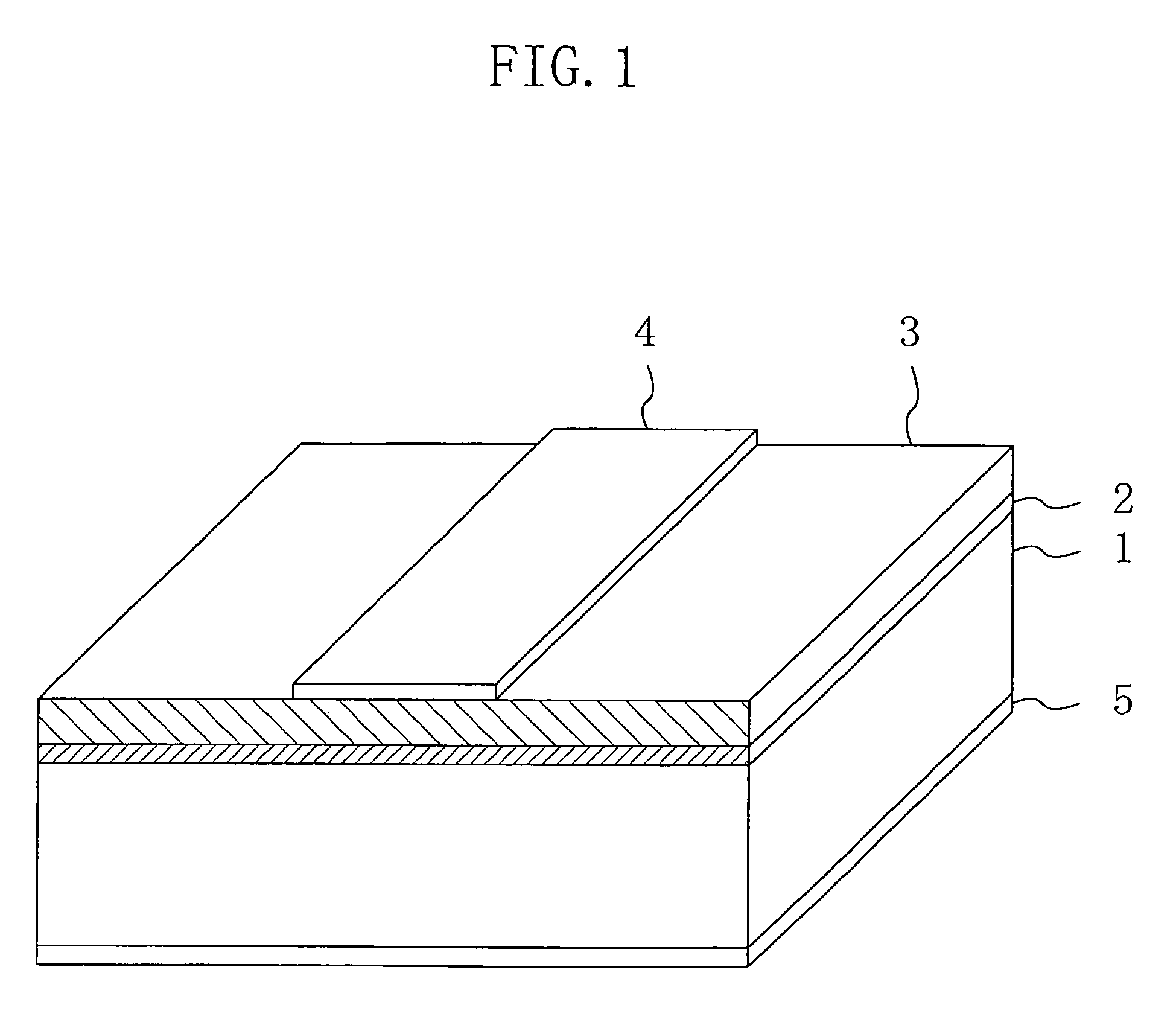
[0039]FIG. 1 partly illustrates the cross-sectional structure of a microwave transmission line according to a first embodiment of the present invention, i.e., a microstrip line. As illustrated in FIG. 1, an approximately 50-nm-thick protective film 2 of silicon oxide (SiO2) serving as a first dielectric film and an approximately 500-nm-thick potential neutralizing film 3 of aluminum oxide (Al2O3) serving as a second dielectric film are successively formed on the principal surface of an approximately 100-μm-thick high-resistivity substrate 1 of high-resistivity p−-type silicon having a majority carrier (hole) density of approximately 1×1013 cm−3 or less.
[0040]An approximately 40-μm-wide strip metal 4 of, for example, gold (Au), aluminum (Al) or the like is formed on the potential neutralizing film 3, and a grounding metal 5 of, for example, gold (Au), alu...
modification 1
[0047](Modification 1 of Embodiment 1)
[0048]A first modification of the first embodiment of the present invention will be described hereinafter with reference to the drawings.
[0049]FIG. 2 partly illustrates the cross-sectional structure of a microwave transmission line according to a first modification of the first embodiment of the present invention, i.e., a microstrip line. Referring to FIG. 2, the same components as those shown in FIG. 1 are designated by the same reference numerals, and thus a description thereof is not given.
[0050]In the first embodiment depicted in FIG. 1, the potential neutralizing film 3 made of aluminum oxide is stacked on the protective film 2 made of silicon oxide. It is also considered that the differences between silicon oxide and aluminum oxide in the temperatures at which they are formed in films and their physical properties provide an imbalance between internal stresses caused in the protective film 2 and the potential neutralizing film 3. In this c...
modification 2
[0054](Modification 2 of Embodiment 1)
[0055]A second modification of the first embodiment of the present invention will be described hereinafter with reference to the drawings.
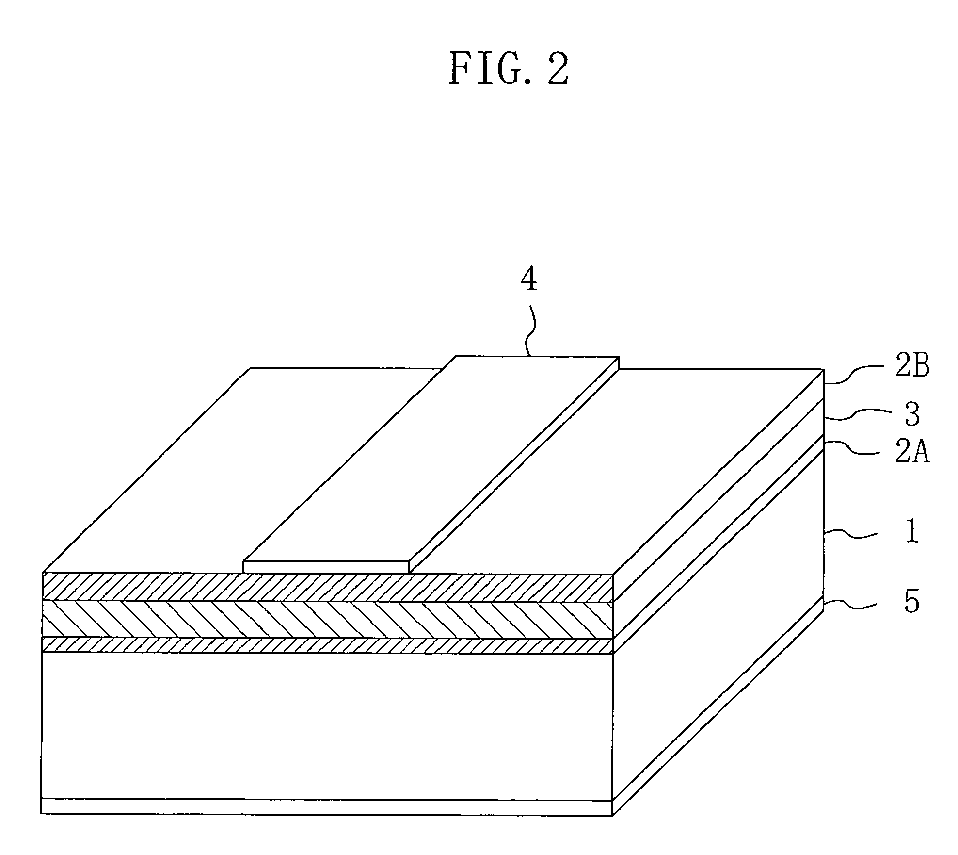
[0056]FIG. 3 partly illustrates the cross-sectional structure of a microwave transmission line according to a second modification of the first embodiment of the present invention, i.e., a microstrip line. Referring to FIG. 3, the same components as those shown in FIG. 1 are designated by the same reference numerals, and thus a description thereof is not given.
[0057]As illustrated in FIG. 3, the microwave transmission line according to the second modification has the following configuration. A first protective film 2A of silicon oxide and a first potential neutralizing film 3A of aluminum oxide are provided between a high-resistivity substrate 1 and a strip metal 4 in this order from the substrate side, and a second protective film 2B of silicon oxide and a second potential neutralizing film 3B of aluminum oxid...
PUM
 Abstract
Description
Claims
Application Information