Method of forming high aspect ratio apertures

a technology of high aspect ratio and aperture, applied in the field of forming apertures, can solve the problem of not allowing free fluorine scavenging to occur

Inactive Publication Date: 2007-01-16
MICRON TECH INC
View PDF23 Cites 15 Cited by
  • Summary
  • Abstract
  • Description
  • Claims
  • Application Information

AI Technical Summary

Benefits of technology

[0026]The present invention provides a process of managing the amount of deposition that occurs in an etch chamber during an etch. The present invention provides a process suitable for use with the Dielectric Etch IPS Centura® system for etching doped silicon dioxide in the form of BPSG and other doped and undoped dielectric films used in integrated circuit fabrication, including, without limitation, SiO2, TEOS, BSG, and PSG, employin

Problems solved by technology

The roof is preferably held at a temperature of between about 115° C. and 150° C., whic

Method used


Image

  • Method of forming high aspect ratio apertures
  • Method of forming high aspect ratio apertures
  • Method of forming high aspect ratio apertures

Examples


example 1

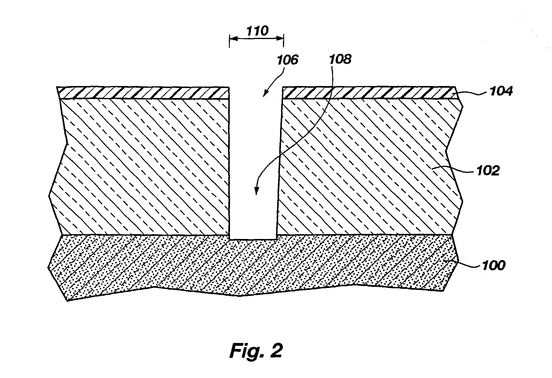
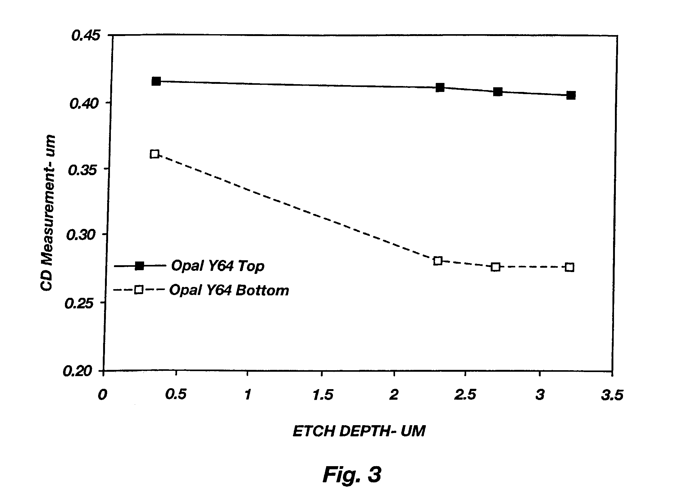
[0049]For the sake of convenience, EXAMPLE 1 will be described with respect to FIG. 2. A 200 mm silicon test wafer 100, having a 2.2 μm thick BPSG layer 102, was inserted in the etch chamber of an IPS system. An I-line resist 104 had been previously applied and patterned to define 0.4 μm diameter exposed areas 106 on the upper surface of the BPSG for contact formation therethrough into the underlying substrate silicon. The IPS system was operated at the most preferred process parameters, as disclosed above, for a period of approximately 210 seconds to conduct a plasma etch, forming contacts 108 of 2.2 μm depth, achieving a 2.6 μm effective etch depth including over-etch of 0.4 μm. Top CD 110 was maintained within 0.01 μm of the 0.4 μm diameter exposed area 106, and the contact 108 exhibited a vertical, only slightly tapered, but very acceptable, profile. CD control was measured by comparing the CD of a 30 second etch to that of the full 210 second etch.

[0050]FIG. 3 is a graphical re...

example 2

[0051]Referring to FIG. 4, a 200 mm silicon test wafer 100 with BPSG layer 102 thereover as in EXAMPLE 1 was plasma etched in an IPS system in accordance with the method as described therein. In a variation of EXAMPLE 1, however, the flow of CH2F2 was reduced to zero at the latter part of the etch (in this case, for the last 50 seconds of the etch). This variation of the inventive method may exhibit a discernable dimple or “punch”112 (shown in broken lines), into the substrate silicon test wafer 100 while maintaining top CD 110 and an acceptable contact profile.

[0052]Referring to FIG. 5, the same method is used to etch through both the BPSG layer 102 and a nitride film 114 to a word line 116 thereunder. The method resulted in reduced taper in the feature as it passed through the nitride film 114 above the word line 116. This two-step process results in a desirable, larger contact dimension 118 (i.e., diameter).

[0053]The inventive etch process described for the first embodiment of th...


PUM

PropertyMeasurementUnit
Temperatureaaaaaaaaaa

Abstract

A plasma etch process for etching BPSG employing two primary etchants at low flows and pressures, and a relatively low temperature environment within the etch chamber, which includes a fluorine scavenger in the form of silicon. The two primary etchant gases are CHF3 and CH2F2, delivered at flow rates on the order of between about 10 and 40 sccm for CHF3 and between about 10 and 40 sccm for CH2F2. Small quantities, on the order of 10 sccm or less, of other gases such as C2HF5 and CF4 may be added.

Description

CROSS-REFERENCE TO RELATED APPLICATIONS[0001]This application is a continuation of application Ser. No. 10 / 060,436, filed Jan. 29, 2002, now U.S. Pat. No. 6,610,212, issued Aug. 26, 2003, which is a continuation of application Ser. No. 09 / 619,101, filed Jul. 19, 2000, now U.S. Pat. No. 6,342,165, issued Jan. 29, 2002, which is a continuation of application Ser. No. 09 / 099,090, filed Jun. 17, 1998, now U.S. Pat. No. 6,123,862, issued Sep. 26, 2000, which claims the benefit of U.S. Provisional Application No. 60 / 082,908, filed Apr. 24, 1998.BACKGROUND OF THE INVENTION[0002]1. Field of the Invention[0003]The present invention relates to a method of forming apertures in a dielectric layer overlying a substrate of semiconductor material and, more specifically, to a method of forming high aspect ratio contact apertures through doped silicon dioxide using an inductively coupled etcher.[0004]2. State of the Art[0005]The semiconductor industry's persistence in development efforts to achieve ...

Claims


Application Information

Patent Timeline
IPC IPC(8): H01L21/3065C03C15/00C03C25/68H01L21/308H05H1/46H01L21/302H01L21/311H01L21/768
CPCH01L21/31116C23C14/34
Inventor DONOHOE, KEVIN G.BECKER, DAVID S.
Owner MICRON TECH INC
Why Eureka
Try Eureka