Heat dissipation for heat generating element of semiconductor device and related method

a heat generating element and semiconductor technology, applied in semiconductor devices, semiconductor/solid-state device details, electrical devices, etc., can solve the problems of substantial heat generation in and near precision resistors, performance of precision resistors, and heat dissipation in semiconductor devices continues to be a challenge, so as to eliminate the loss of current carrying capability in wiring, the effect of reducing the amount of heat transfer

Active Publication Date: 2007-01-23
GLOBALFOUNDRIES US INC
View PDF17 Cites 34 Cited by
  • Summary
  • Abstract
  • Description
  • Claims
  • Application Information

AI Technical Summary

Benefits of technology

[0006]The invention includes a structure and method for heat dissipation relative to a heat generating element in a semiconductor device. The structure includes a plurality of heat transmitting lines partially vertically coincidental with the heat generating element, and at least one interconnecting path from each heat transmitting line to a substrate of the semiconductor device. In one embodiment, the heat generating element includes a resistor in a non-first metal level. The invention is compatible with conventional BEOL interconnect schemes, minimizes the amount of heat transfer from the resistor to the surrounding interconnect wiring, thus eliminating the loss of current carrying capability in the wiring.

Problems solved by technology

Heat dissipation in semiconductor devices continues to be a challenge as size continually shrinks.
Unfortunately, the resistance of precision resistors ranges from about 60 to 100 Ohms / square, which under normal operating currents, generates substantial heat in and near the precision resistor.
Higher temperatures limit the performance of the precision resistors and degrade the electromigration performance of surrounding metal, which leads to lower maximum currents and increased complexity and cost to produce semiconductor microprocessors.
Since no metal is allowed above or below the precision resistors, only heat transmission through typically very poor heat conductive dielectrics is possible.

Method used


Image

  • Heat dissipation for heat generating element of semiconductor device and related method
  • Heat dissipation for heat generating element of semiconductor device and related method
  • Heat dissipation for heat generating element of semiconductor device and related method

Examples


Embodiment Construction

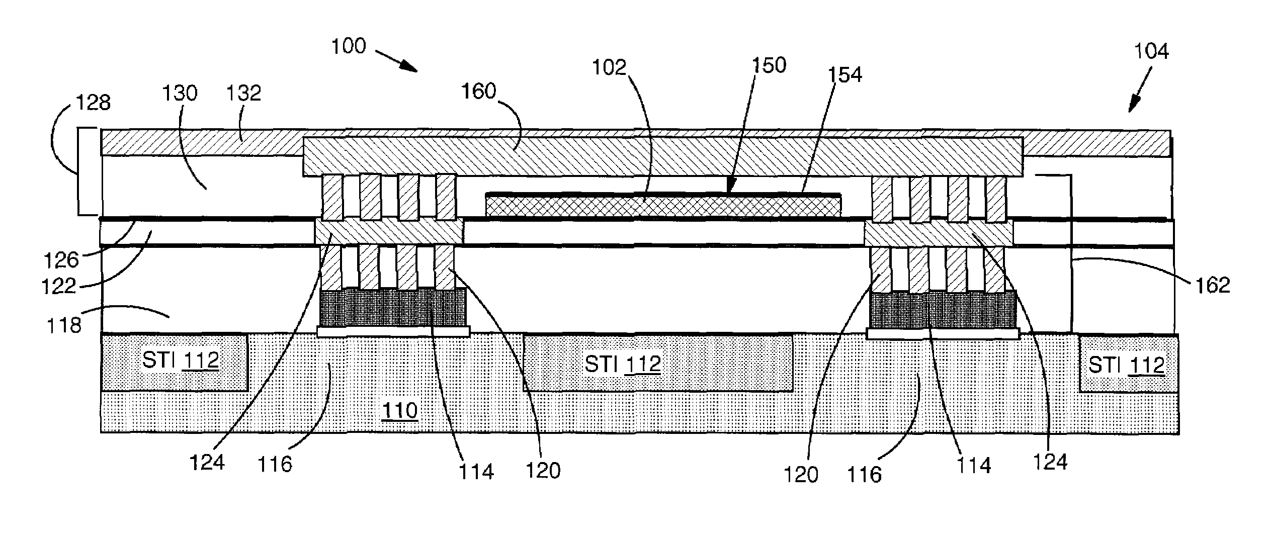
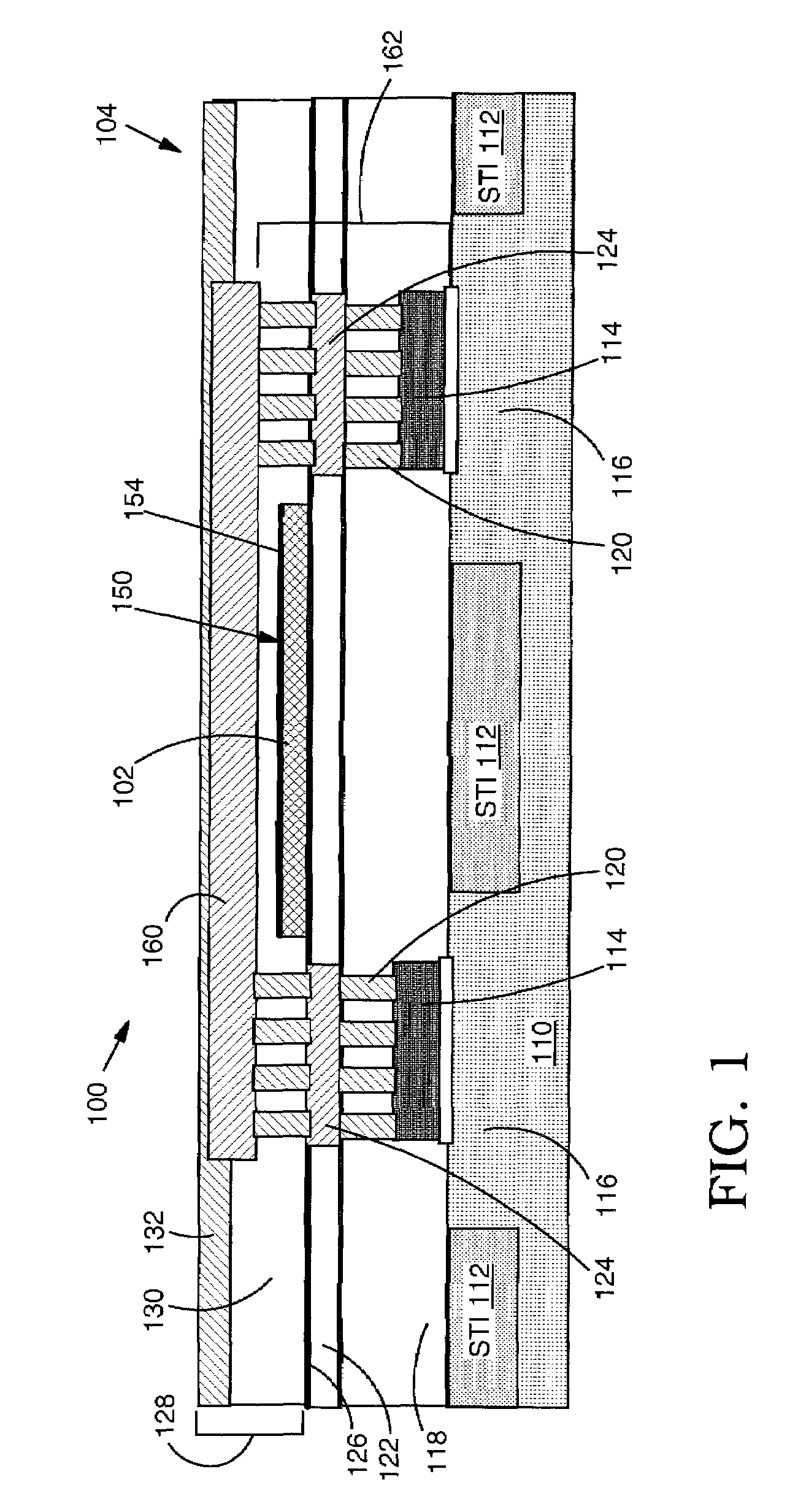
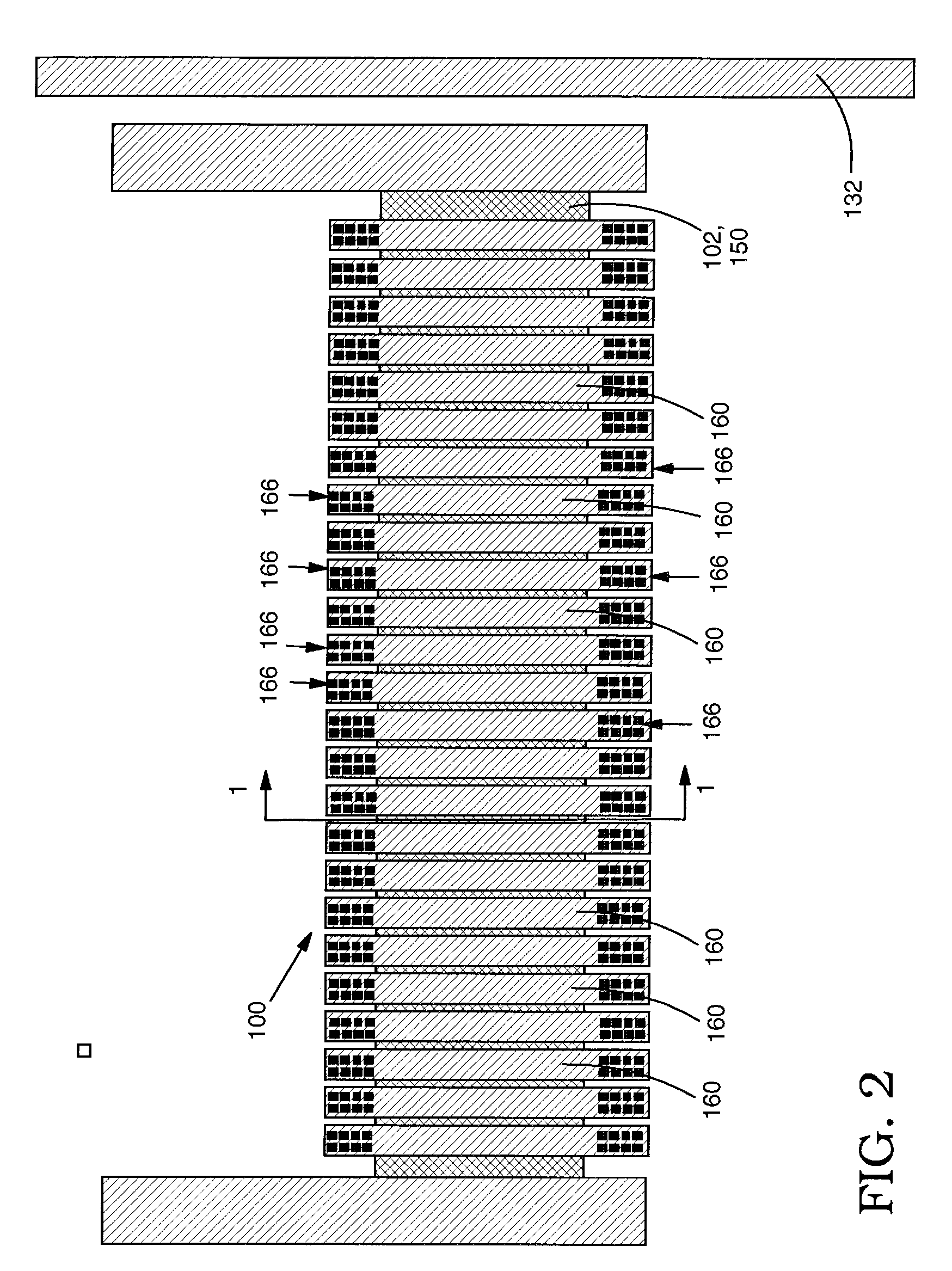
[0019]With reference to the accompanying drawings, FIG. 1 shows a cross-sectional view of a structure 100 for heat dissipation relative to a heat generating element 102 in a semiconductor device 104. FIGS. 2, 4 and 5 show a plan view of structure 100 relative to first, second and third embodiments of a heat generating element 102, 202, 302, respectively. The semiconductor device 104 may include a conventional structure such as a silicon substrate 110 including shallow trench isolations (STI) 112, e.g., of silicon dioxide (SiO2), a polysilicon gate structure 114 over silicon region 116, a dielectric cap 118 (e.g., tetraethyl orthosilicate (Si(OC2H5)4)(TEOS) or boro-phospho-silicate glass (BPSG)), contact vias 120, a first back-end-of-line dielectric 122, conducting lines 124, and a sealing dielectric cap layer 126. Back-end-of-line metal layers 128 (only one shown for clarity) may include, for example, a typical dielectric 130, conducting lines 132 or any other conventional structure...


PUM


Abstract

A structure and method are disclosed for heat dissipation relative to a heat generating element in a semiconductor device. The structure includes a plurality of heat transmitting lines partially vertically coincidental with the heat generating element, and at least one interconnecting path from each heat transmitting line to a substrate of the semiconductor device. In one embodiment, the heat generating element includes a resistor in a non-first metal level. The invention is compatible with conventional BEOL interconnect schemes, minimizes the amount of heat transfer from the resistor to the surrounding interconnect wiring, thus eliminating the loss of current carrying capability in the wiring.

Description

BACKGROUND OF THE INVENTION[0001]1. Technical Field[0002]The present invention relates generally to semiconductor devices, and more particularly, to heat dissipation for a heat generating element in a semiconductor device.[0003]2. Related Art[0004]Heat dissipation in semiconductor devices continues to be a challenge as size continually shrinks. One particular element in semiconductor device structures that presents challenges relative to heat dissipation is a precision resistor, which represents an important element in microprocessor technology. For example, precision resistors are used to reduce parasitic capacitance in conventional advanced logic circuits. For technologies at 90 nm and smaller, refractory metal resistors embedded in the back-end-of-the-line (BEOL) (i.e., after first metal) are being used instead of polysilicon or single crystalline resistors due to their better resistance tolerance, lower thermal coefficient of resistance (TCR) and lower parasitic capacitance to t...

Claims


Application Information

Patent Timeline
Patent Type & Authority Patents(United States)
IPC IPC(8): H01L23/34
CPCH01L23/3677H01L23/5228H01L2924/0002H01L2924/00
Inventor CHINTHAKINDI, ANIL K.CLEVENGER, LAWRENCE A.LEE, TOM C.MATUSIEWICZ, GERALDMURRAY, CONAL E.YANG, CHIH-CHAO
Owner GLOBALFOUNDRIES US INC
Why Eureka
Try Eureka