Beam homogenizer, laser irradiation apparatus, and method for manufacturing semiconductor device

a laser irradiation and laser irradiation technology, applied in semiconductor lasers, instruments, record information storage, etc., can solve the problem of insufficient homogenization of the energy distribution of the beam spot at the exit surface of the optical element, and achieve the effect of suppressing inhomogeneous crystallinity, improving crystallinity, and keeping the shape of the beam spot stably

Active Publication Date: 2007-01-30
SEMICON ENERGY LAB CO LTD
View PDF51 Cites 27 Cited by
  • Summary
  • Abstract
  • Description
  • Claims
  • Application Information

AI Technical Summary

Benefits of technology

[0041]When the beam homogenizer including the optical element that homogenizes the energy distribution of the laser beam and that has a curved shape in its entrance surface where the laser beam is incident for forming a rectangular beam spot disclosed in the present invention is used, it is possible to form a rectangular beam spot having homogeneous energy distribution on the irradiated surface. Moreover, since the position and the energy distribution of the beam spot formed on the irradiated surface are not easily affected by the oscillation condition of the laser oscillator, it is possible to keep the shape of the beam spot stably.
[0042]When the rectangular beam spot emitted from the laser irradiation apparatus using the beam homogenizer of the present invention is scanned on a semiconductor film in a direction of its short side, it is possible to suppress the inhomogeneous crystallinity due to the inhomogeneous energy distribution of the beam spot and to improve the homogeneity of the crystallinity in the surface of the substrate. Moreover, according to the present invention, the laser irradiation apparatus can obtain the high stability. Furthermore, since it is possible to do the maintenance more easily, the running cost can be reduced. With the present invention applied to the mass production line of the poly-silicon TFT, a TFT having high operating characteristic uniformly can be manufactured efficiently. Moreover, when the poly-silicon TFT manufactured by the present invention is applied to a liquid crystal display device and a light-emitting device using a light-emitting element typified by an EL element, it is possible to manufacture a display device having almost no display unevenness.

Problems solved by technology

Therefore, the energy distribution of the beam spot at the exit surface of the optical element is not sufficiently homogenized.

Method used


Image

  • Beam homogenizer, laser irradiation apparatus, and method for manufacturing semiconductor device
  • Beam homogenizer, laser irradiation apparatus, and method for manufacturing semiconductor device
  • Beam homogenizer, laser irradiation apparatus, and method for manufacturing semiconductor device

Examples


embodiment 1

[Embodiment 1]

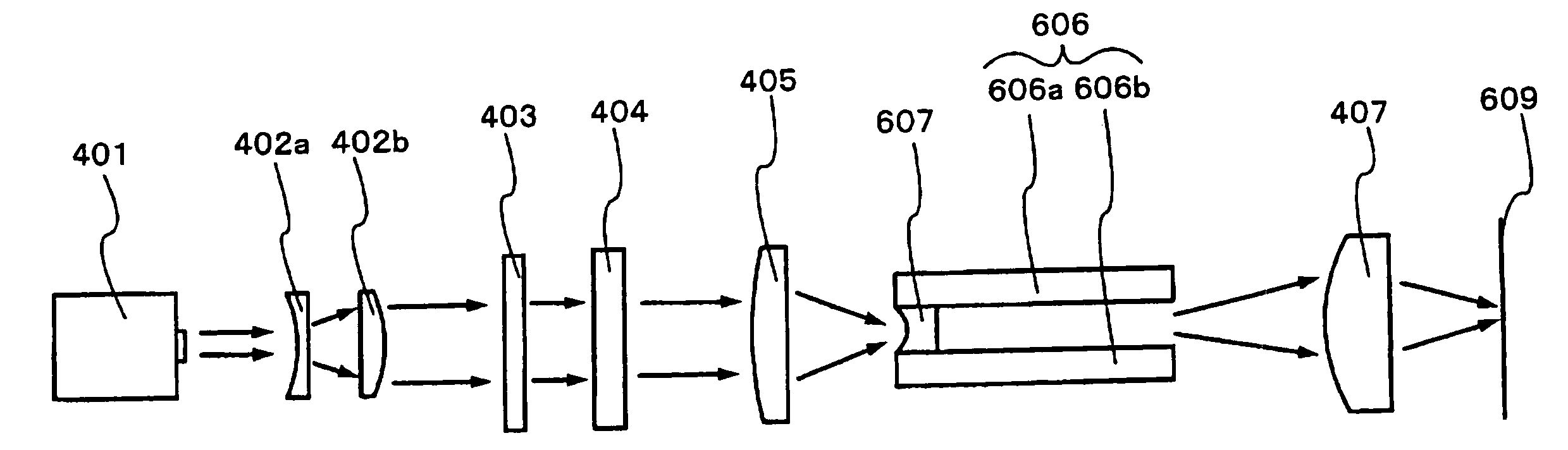
[0088]An example of an optical system used in the present embodiment is explained with reference to FIGS. 4A and 4B. A side view of FIG. 4B is explained first. A laser beam emitted from a XeCl excimer laser oscillator 401 propagates in a direction indicated by an arrow in FIGS. 4A and 4B. First, the laser beam is expanded by spherical lenses 402a and 402b. The spherical lenses 402a and 402b are not necessary when the beam spot emitted from the laser oscillator 401 is sufficiently large. It is noted that the lenses and the light pipe that has a curved shape in its entrance surface for homogenizing the energy distribution of the laser beam shown in the present embodiment are made of synthetic quartz having high transmittance and resistance to the XeCl excimer laser.

[0089]The direction of the long side herein described mean the direction of the long side of the rectangular beam spot formed on an irradiated surface 408. The direction of the short side herein described mean...

embodiment 2

[Embodiment 2]

[0096]The present embodiment explains an example of an optical system different from that described above. FIGS. 6A and 6B show the example of the optical system explained in this embodiment. In addition, the lenses shown in the present embodiment are made of synthetic quartz having high transmittance and resistance to the XeCl excimer laser.

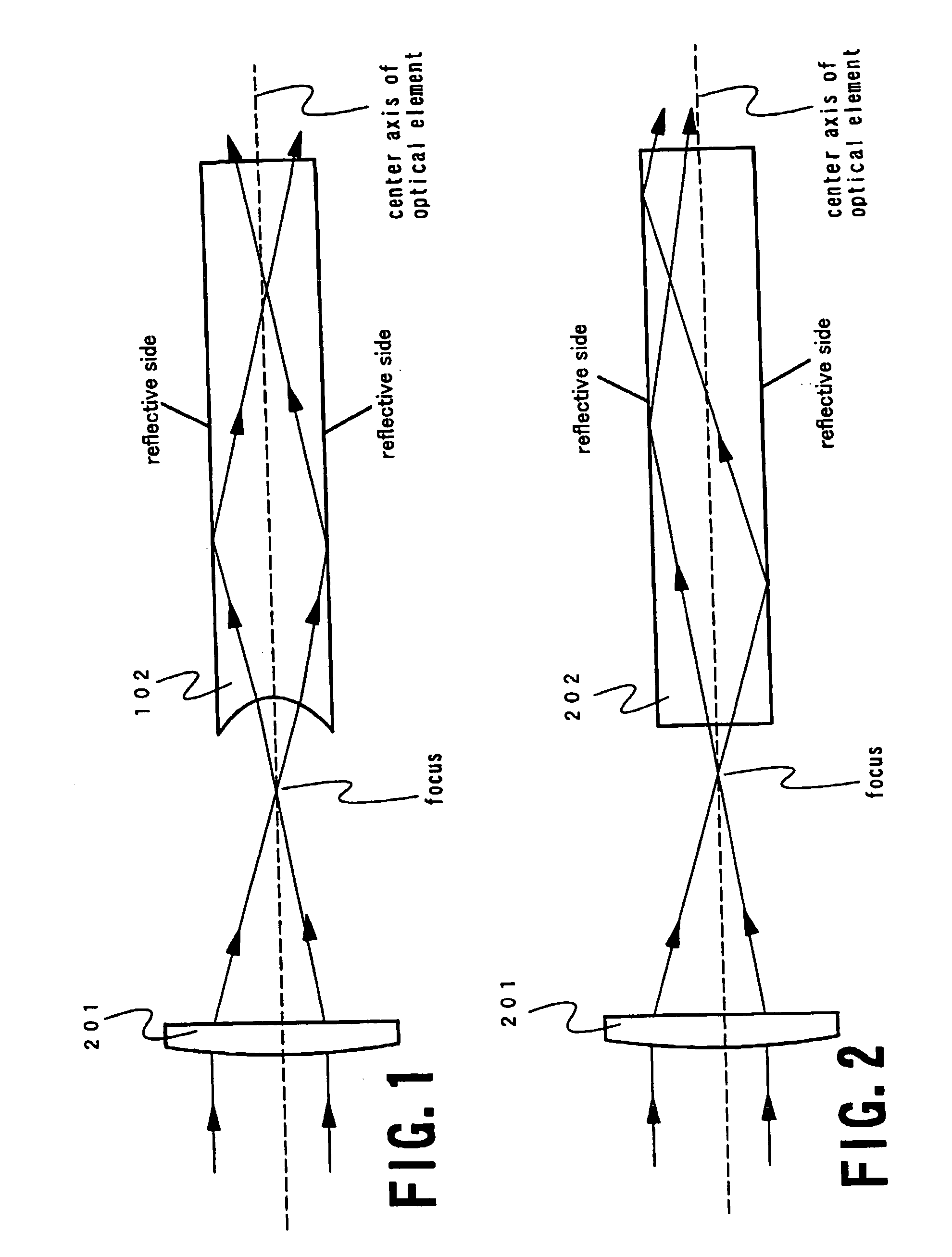
[0097]In FIGS. 6A and 6B, the laser beam travels in the same optical path as that shown in FIGS. 4A and 4B in the embodiment 1 except for an optical element 606 that has a curved shape in its entrance surface for homogenizing the energy distribution of the laser beam. The optical element 606 has a pair of reflection planes provided oppositely as well as the light pipe 406. The light pipe 406 in FIGS. 4A and 4B has curvature in the entrance surface thereof and is made of synthetic quartz having a refractive index of approximately 1.486 to the XeCl excimer laser. The laser beam incident into the light pipe 406 is totally reflected in...

embodiment 3

[Embodiment 3]

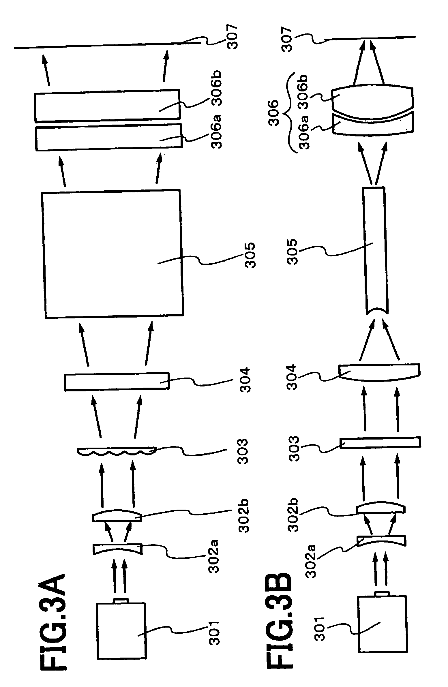
[0103]This embodiment explains an example of an optical system different from that described above. FIGS. 7A and 7B show the example of the optical system explained in this embodiment. It is noted that the lenses shown in the present embodiment are made of synthetic quartz having high transmittance and resistance to the XeCl excimer laser.

[0104]In FIGS. 7A and 7B, the laser beam travels in the same optical path as that shown in FIGS. 6A and 6B in the embodiment 2 except for a cylindrical lens 707. An optical element 706 has a pair of reflection planes provided oppositely as well as the optical element 606. In FIGS. 6A and 6B, the laser beam incident into the optical element 606 is expanded in a direction of the short side of the rectangular beam spot by a concave cylindrical lens 607 provided in the vicinity of the entrance of the optical element 606. On the other hand, in FIGS. 7A and 7B, the laser beam incident into the optical element 706 is focused by a convex cyli...


PUM

PropertyMeasurementUnit
aspect ratioaaaaaaaaaa
lengthaaaaaaaaaa

Abstract

The energy distribution of the beam spot on the irradiated surface changes due to the change in the oscillation condition of the laser or before and after the maintenance. The present invention provides an optical system for forming a rectangular beam spot on an irradiated surface including a beam homogenizer for homogenizing the energy distribution of the rectangular beam spot on the irradiated surface in a direction of its long or short side. The beam homogenizer includes an optical element having a pair of reflection planes provided oppositely for reflecting the laser beam in the direction where the energy distribution is homogenized and having a curved shape in its entrance surface. The entrance surface of the optical element means a surface of the optical element where the laser beam is incident first.

Description

BACKGROUND OF THE INVENTION[0001]1. Field of the Invention[0002]The present invention relates to a beam homogenizer to homogenize energy distribution of a beam spot on an irradiated surface in a particular region. Moreover, the present invention also relates to a laser irradiation apparatus using the beam homogenizer. Furthermore, the present invention relates to a method for manufacturing a semiconductor device using the laser irradiation apparatus.[0003]2. Related Art[0004]In recent years, a technique has been extensively researched in which the laser annealing is performed to a non-single crystal semiconductor film (the non-single crystal semiconductor includes an amorphous semiconductor and a semiconductor having crystallinity such as poly-crystal or micro-crystal, which is not single crystal) formed over an insulating substrate such as a glass substrate. It is noted that the laser annealing described herein indicates a technique to recrystallize an amorphous layer or a damaged ...

Claims


Application Information

Patent Timeline
Patent Type & Authority Patents(United States)
IPC IPC(8): H01L21/00G02B27/09G11B11/00H01S3/00H01S3/13H01S5/00
CPCG02B27/0994H01L21/02678H01L21/02595B82Y20/00H01S3/005
Inventor MORIWAKA, TOMOAKI
Owner SEMICON ENERGY LAB CO LTD
Why Eureka
Try Eureka