Arrangement and method for ESD protection

a technology of esd protection and arrangement, applied in the direction of circuit arrangement, semiconductor device details, semiconductor/solid-state device details, etc., can solve the problems of large leakage current of the structure, insufficient voltage range of the structure to cover all product needs, and choice of internal protection structures

Active Publication Date: 2007-01-30
VLSI TECH LLC
View PDF4 Cites 11 Cited by
  • Summary
  • Abstract
  • Description
  • Claims
  • Application Information

AI Technical Summary

Problems solved by technology

This LNPN transistor may turn on and undesirably provide an alternate ESD path.
The voltage range of this structure is not sufficient to cover all the product needs.
Bipolar transistors assembled in cascade are one of the solutions but these structures exhibit an important leakage current.
An important difficulty in implementing findings of such a study is in the choice of internal protection structures.

Method used


Image

  • Arrangement and method for ESD protection
  • Arrangement and method for ESD protection
  • Arrangement and method for ESD protection

Examples


Embodiment Construction

)

[0020]The Electro-Static Discharge (ESD) problem is one of the first causes of redesign for integrated circuits after ‘first silicon’. A wide range of solutions is already existing but they are each dedicated to protect only one kind of circuit. Hence, different ESD structures have to be developed for each application. In consequence, the ESD protection structures must be redefined and redeveloped for each technology and application.

[0021]Another point which has to be considered is the current absorption during the non-operating mode of the protection system.

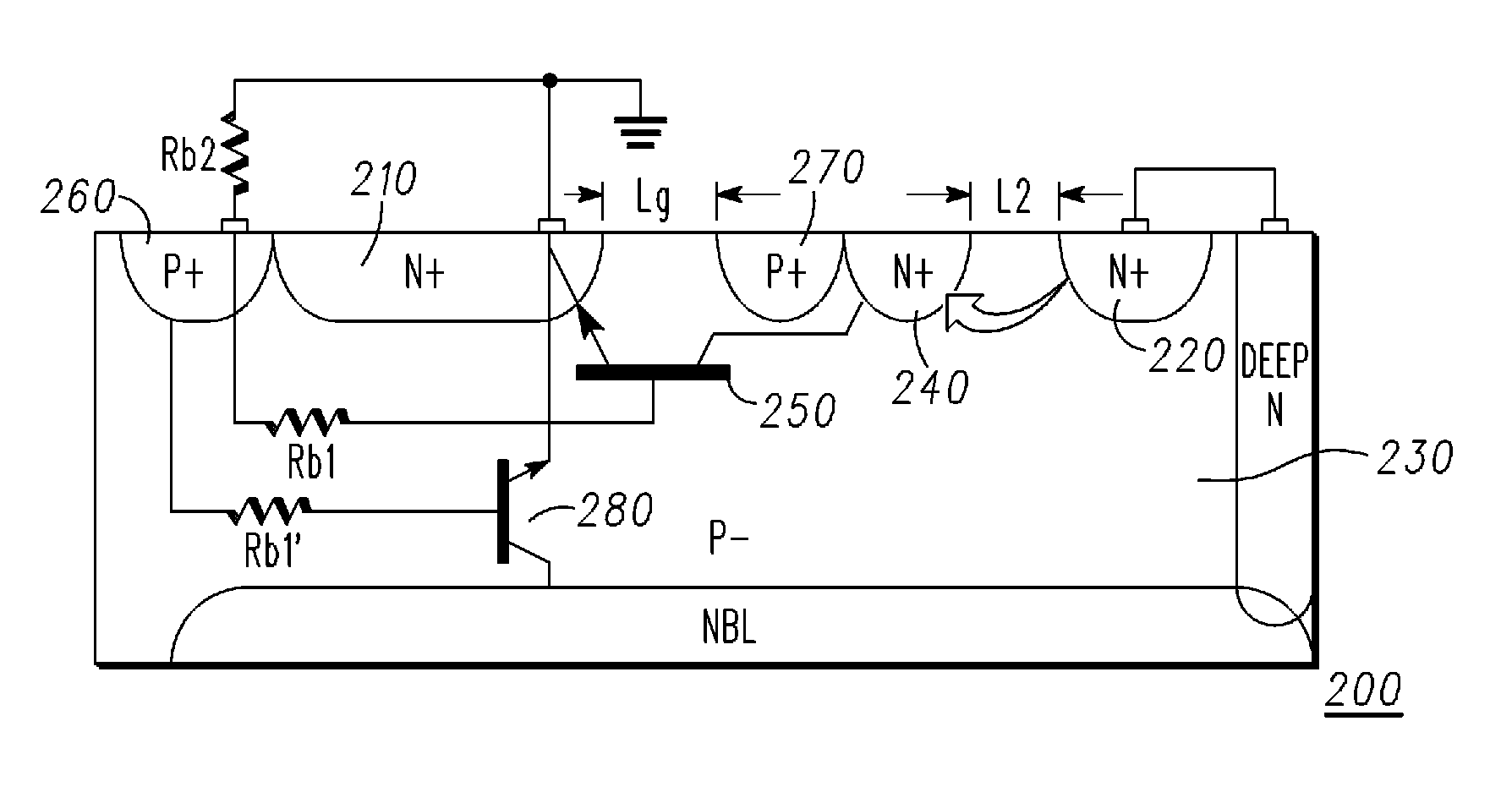
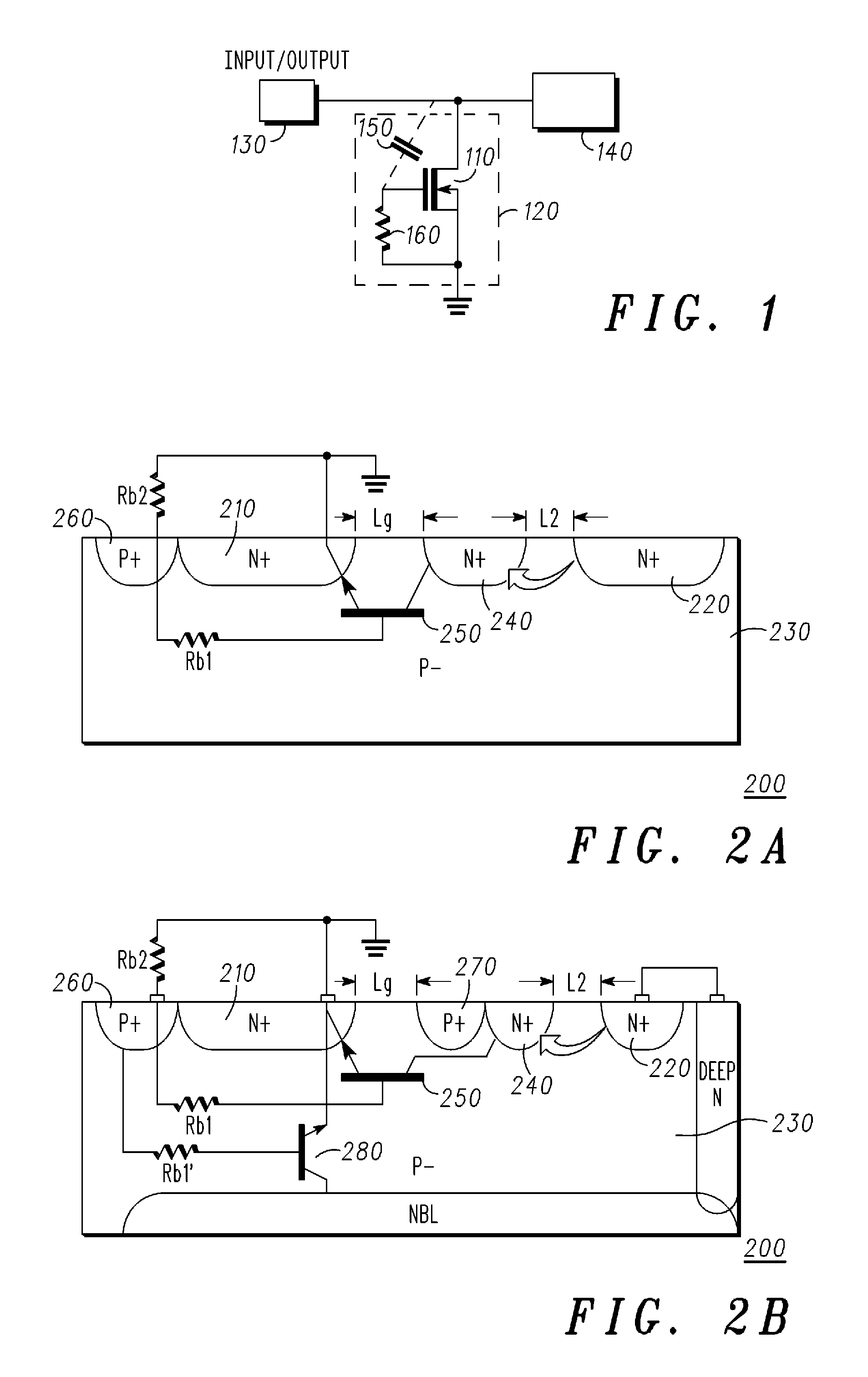
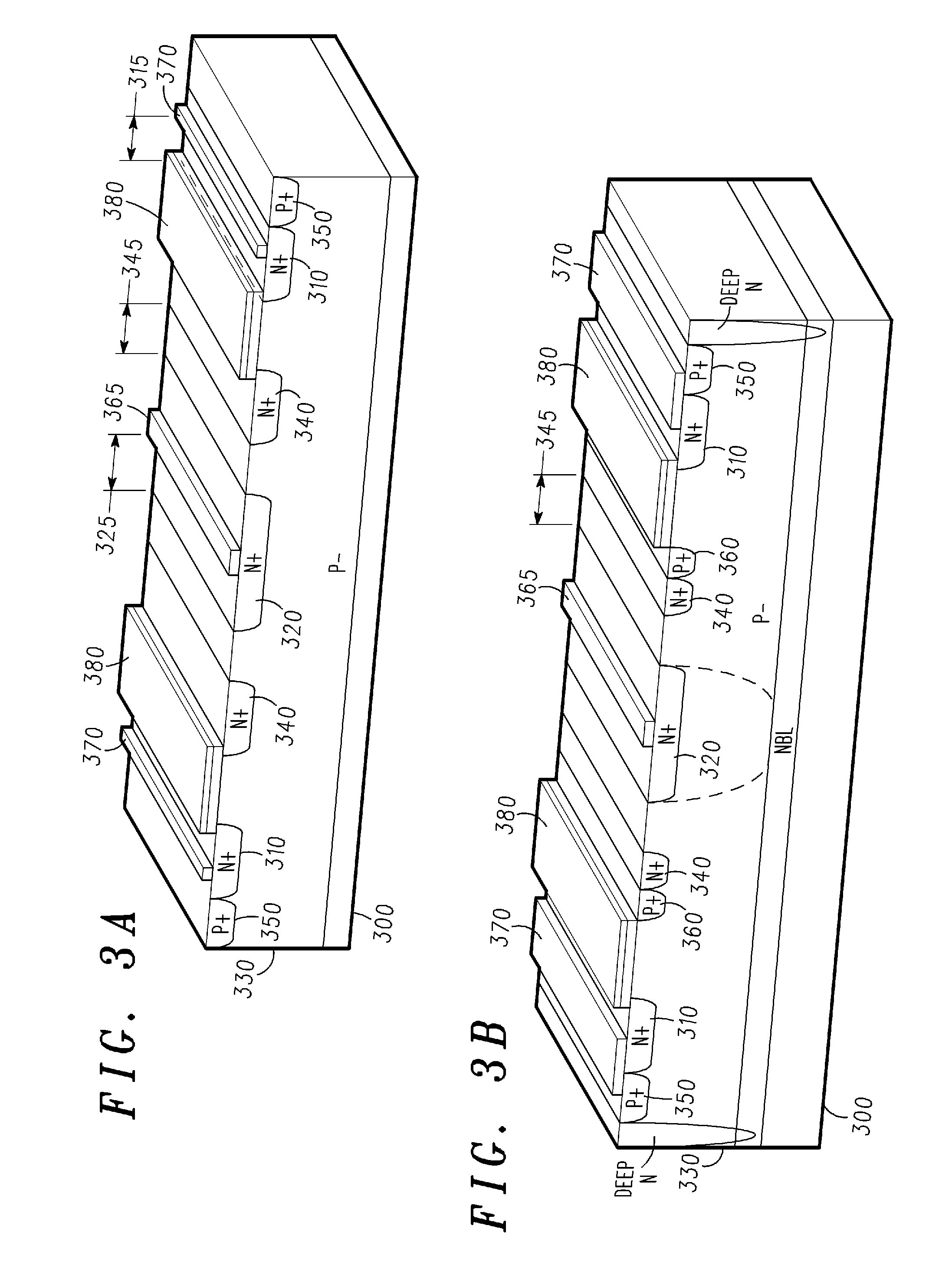
[0022]As will be described in greater detail below, the present invention allows an ESD protection structure permitting a scalable level of voltage protection (scalable Vt1) without changing the number of external components and may be based on NMOS of PMOS devices and may require only one different photloythographic mask to introduce additional n+ and / or p+ apertures in a DRIFT area.

[0023]Such a structure could be used to prot...


PUM


Abstract

An arrangement (200) and method for scalable ESD protection of a semiconductor structure (140), a protection structure (120) providing a discharge transistor (110) path from an input / output node (130) to ground or another node if a threshold voltage is reached, wherein the discharge transistor is a self-triggered transistor having collector / drain (220) and emitter / source (210) regions, and a base / bulk region (260) having one or more floating regions (240) between the collector / drain (220) and emitter / source (210) regions. The floating region (N or P) modulates the threshold voltage Vtl for ESD protection. Vtl can be adjusted by shifting the floating region location. Splitting of the electric field into two parts reduces the maximum of the electric field. Vt1 can be adjusted volt-by-volt to suit application needs. ESD capability is increased by better current distribution in the silicon. This provides the advantages of reduced die size, faster time-to-market, less redesign cost, and better ESD performance.

Description

FIELD OF THE INVENTION [0001]This invention relates to electrostatic discharge (ESD) protection, and particularly to scalable ESD protection for integrated circuits.BACKGROUND OF THE INVENTION [0002]The Electro-Static Discharge (ESD) problem is one of the first causes of redesign, after initial design and fabrication (e.g., ‘first silicon’), for integrated circuits. A wide range of ESD solutions already exists but they are dedicated to protect only one kind of circuit. Hence, different ESD structures have to be developed for each application. In consequence, the ESD protection structures must be redefined and redeveloped for each technology and application.[0003]Another point which has to be considered is the current absorption during the non-operating mode of the protection system.[0004]An effective ESD protection has to be able to support ESD-HBM (Human Body Model minimum 2KV) and -MM (Machine Model minimum 200V) stresses with a minimum current consumption in normal operating mode...

Claims


Application Information

Patent Timeline
Patent Type & Authority Patents(United States)
IPC IPC(8): H01L23/60H01L27/02
CPCH01L27/0259H01L29/735H01L27/0266
Inventor ZECRI, MICHELBESSE, PATRICENOLHIER, NICOLAS
Owner VLSI TECH LLC
Why Eureka
Try Eureka