High frequency switching circuit and semiconductor device

a high-frequency switching and semiconductor technology, applied in the direction of pulse automatic control, waveguide type devices, pulse techniques, etc., can solve the problems of long time for the fets to completely turn, take time, and rounded rising edge of output waveforms, and achieve the effect of superior high-frequency switching circuits

Inactive Publication Date: 2007-02-06
COLLABO INNOVATIONS INC
View PDF19 Cites 75 Cited by
  • Summary
  • Abstract
  • Description
  • Claims
  • Application Information

AI Technical Summary

Benefits of technology

[0032]As having been described above, according to the present invention, the drain control voltages are individually applied to the drain terminal or the source terminal of the FET, and the voltage according to the electric power value of the high frequency signal supplied to the switching circuit section is supplied as the gate control voltage and the drain control voltage, thereby making it possible to provide a superior high frequency switching circuit and a semiconductor device which do not cause a waveform to be rounded.

Problems solved by technology

Incidentally, since an excessive reverse bias is applied to gate-source and gate-drain of each of off-state FETs for a long time, it takes time for the FETs to become an on-state from an off-state.
As a result, there has been a problem that a rising edge of an output waveform is rounded.
Thus, in order to achieve an off-state, a high reverse bias state is maintained, as a result, there causes a problem that it takes long time for the FETs to completely turn on when changing to an on-state next, thereby generating a phenomenon that a rising edge of a transmission waveform is rounded.

Method used


Image

  • High frequency switching circuit and semiconductor device
  • High frequency switching circuit and semiconductor device
  • High frequency switching circuit and semiconductor device

Examples


first embodiment

(First Embodiment)

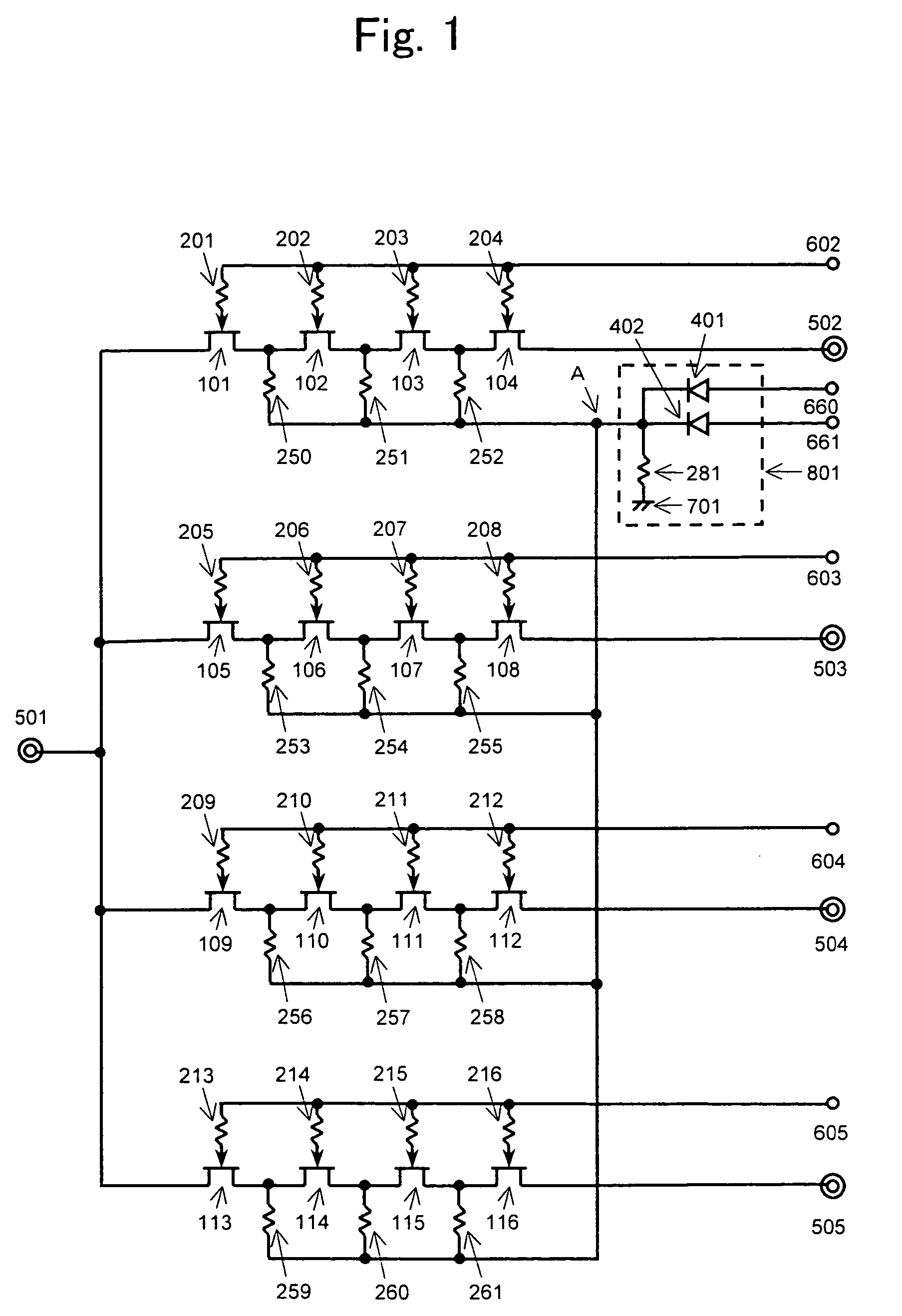
[0044]FIG. 1 shows a configuration of a high frequency switching circuit of a first embodiment of the present invention. In FIG. 1, reference numerals 101 through 116 represent depletion type field effect transistors (henceforth referred to as FET) which configure four switching circuit sections. Reference numerals 201 through 216 represent resistance elements. Reference numerals 250 through 261 represent resistance elements. Reference numeral 281 represents a resistance element. Reference numeral 501 represents a first input / output terminal connected to, for example an antenna. Reference numeral 502 represents a second input / output terminal connected to, for example a first transmitting circuit section. Reference numeral 503 represents a third input / output terminal connected to, for example a second transmitting circuit section. Reference numeral 504 represents a fourth input / output terminal connected to, for example a first receiving circuit section. Reference nu...

second embodiment

(Second Embodiment)

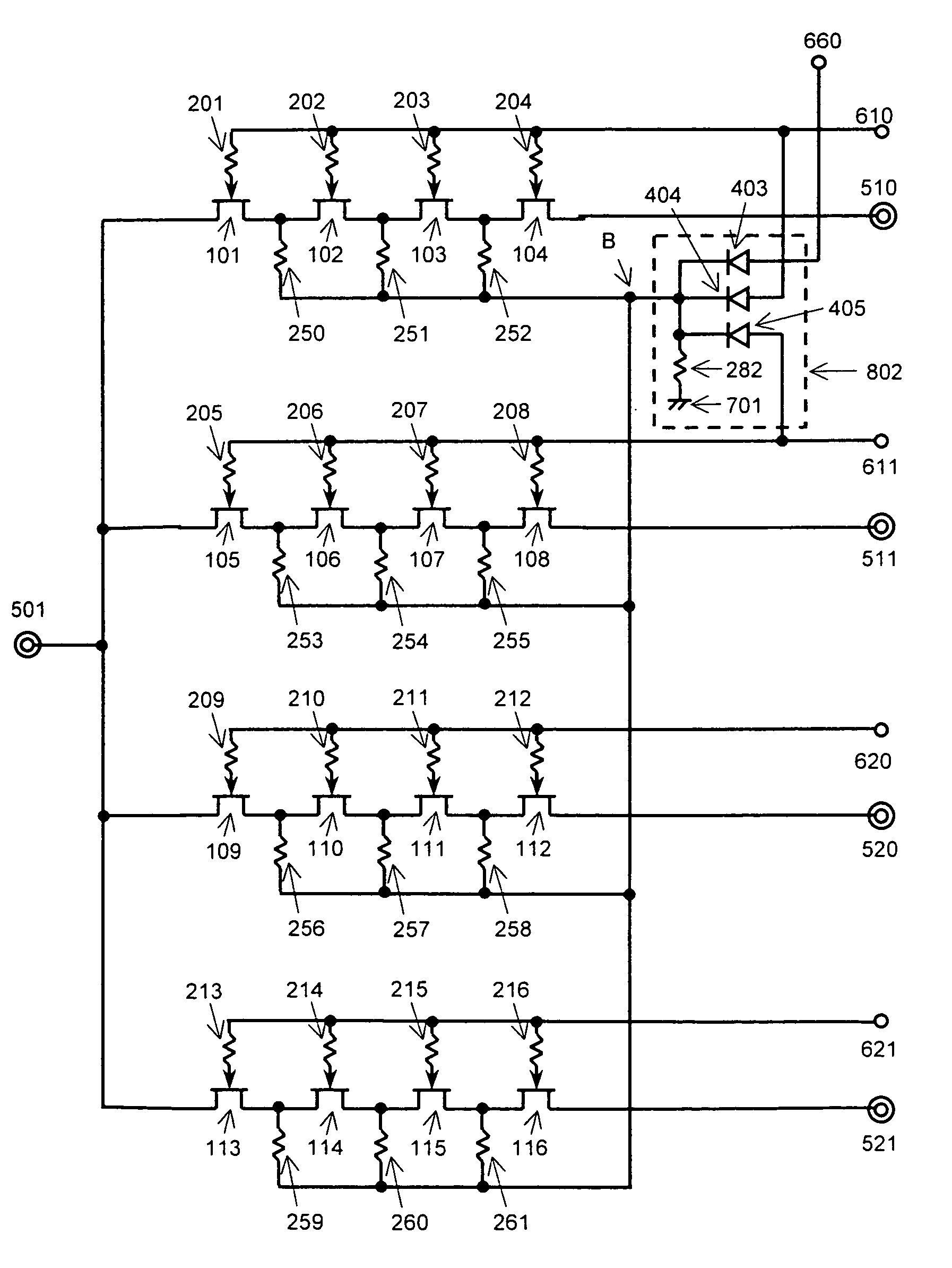
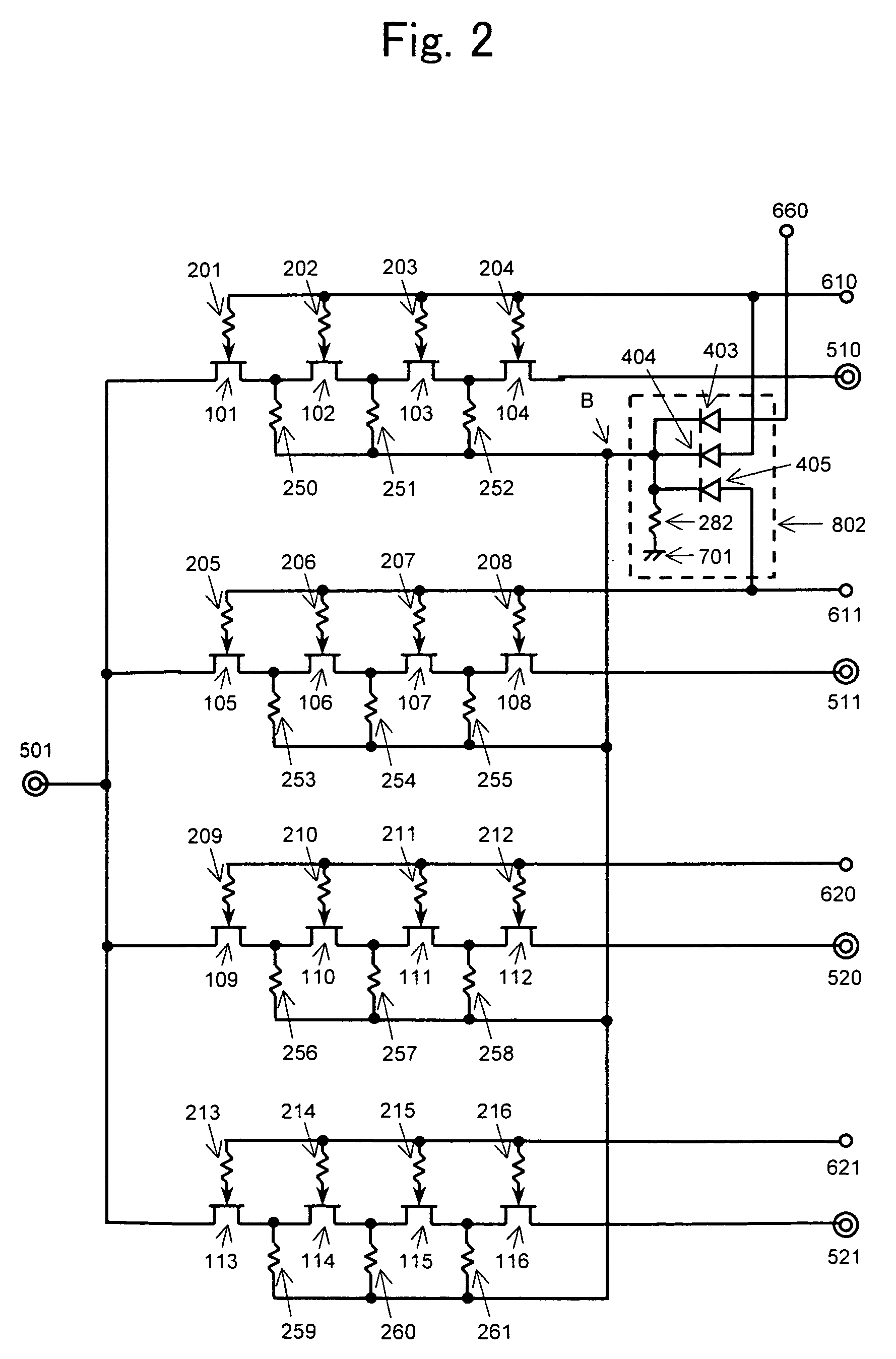
[0063]FIG. 2 shows a configuration of a high frequency switching circuit of a second embodiment of the present invention. In FIG. 2, reference numerals 101 through 116 represent FETs which configure four switching circuit sections. Reference numerals 201 through 216 represent resistance elements. Reference numerals 250 through 261 represent resistance elements. Reference numeral 282 represents a resistance element. Reference numerals 403 through 405 represent diodes which configure an OR circuit. Reference numeral 501 represents an input / output terminal connected to, for example an antenna. Reference numeral 510 represents a first transmission terminal connected to a first transmitting circuit section. Reference numeral 511 represents a second transmission terminal connected to a second transmitting circuit section. Reference numeral 520 represents a first reception terminal connected to a first receiving circuit section. Reference numeral 521 represents a second ...

third embodiment

(Third Embodiment)

[0086]FIG. 4 shows a configuration of a high frequency switching circuit of a third embodiment of the present invention. In FIG. 4, reference numerals 101 through 116 represent FETs which configure four switching circuit sections. Reference numerals 201 through 216 represent resistance elements. Reference numerals 250 through 261 represent resistance elements. Reference numeral 290 represents a resistance element. Reference numerals 406 and 407 represent diodes which configure an OR circuit. Reference numeral 501 represents an input / output terminal connected to, for example an antenna. Reference numeral 510 represents a first transmission terminal connected to a first transmitting circuit section. Reference numeral 511 represents a second transmission terminal connected to a second transmitting circuit section. Reference numeral 520 represents a first reception terminal connected to a first receiving circuit section. Reference numeral 521 represents a second recept...


PUM


Abstract

Four switching circuit sections consisting of four FETs connected in series are provided between a plurality of input / output terminals which output and input a high frequency signal. Gate control voltages are individually applied to gate terminals of four FETs, respectively, so that an on-state and an off-state are achieved. Further drain control voltages are individually applied to drain terminals or source terminals of the FET in each switching circuit section, and a voltage according to an electric power value of the high frequency signal supplied to each of switching circuit sections is supplied as the gate control voltage and the drain control voltage.

Description

BACKGROUND OF THE INVENTION[0001]1. Field of the Invention[0002]The present invention relates to a high frequency switching circuit which performs amplification, switching, or the like of a signal in a mobile communication apparatus or the like, and a semiconductor device in which this high frequency switching circuit is integrated on a semiconductor substrate.[0003]2. Prior Art[0004]A conventional high frequency switching circuit comprises FETs 101 through 104, and 109 through 112, resistance elements 201 through 204, 209 through 212, 250 through 253, and 256 through 259, first through third signal input / output terminals 501 through 503, and first and second control terminals 610, 620 as shown in FIG. 10.[0005]In this high frequency switching circuit, the first control terminal 610 is connected to the third signal input / output terminal 503, and the second control terminal 620 is connected to the second signal input / output terminal 502, so that a bias voltage is applied to the FETs ...

Claims


Application Information

Patent Timeline
Patent Type & Authority Patents(United States)
IPC IPC(8): H03L5/00H03K17/00H03K17/0412H03K17/06H03K17/62H03K17/693
CPCH03K17/693H03K17/04123H03K17/06H03K17/62
Inventor NAKATSUKA, TADAYOSHISUWA, ATSUSHITARA, KATSUSHI
Owner COLLABO INNOVATIONS INC
Why Eureka
Try Eureka